ZHCSCX4A June 2014 – October 2014 ADS8339
PRODUCTION DATA.
- 1 特性
- 2 应用
- 3 说明
- 4 修订历史记录
- 5 Device Family
- 6 Pin Configuration and Functions
- 7 Specifications
- 8 Parametric Measurement Information
- 9 Detailed Description
- 10Application and Implementation
- 11Power-Supply Recommendations
- 12Layout
- 13器件和文档支持
- 14机械封装和可订购信息
9 Detailed Description
9.1 Overview
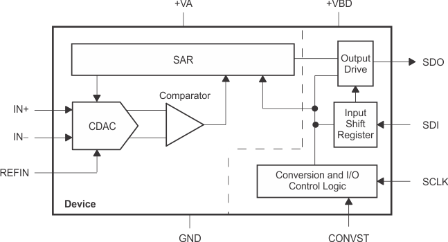
The ADS8339 is a 250-kSPS, low-power, successive-approximation register (SAR), analog-to-digital converter (ADC) that uses an external reference. The architecture is based on charge redistribution, which inherently includes a sample-and-hold function.
The ADS8339 is a single-channel device. The analog input is provided to two input pins: +IN and –IN, where –IN is a pseudo-differential input and has a limited range of ±0.1 V. When a conversion is initiated, the differential input on these pins is sampled on the internal capacitor array. While a conversion is in progress, both the +IN and –IN inputs are disconnected from any internal functions.
The device has an internal clock that is used to run the conversion. Therefore, the conversion requires a fixed amount of time. After a conversion is completed, the device reconnects the sampling capacitors to the +IN and –IN pins and the device is in the acquisition phase. During this phase, the device is powered down and conversion data can be read.
The device digital output is available in SPI-compatible format. The device easily interfaces with microprocessors, digital signal processors (DSPs), or field-programmable gate arrays (FPGAs).
9.2 Functional Block Diagram
9.3 Feature Description
9.3.1 Analog Input
When the converter samples the input, the voltage difference between the +IN and –IN inputs is captured on the internal capacitor array. The differential signal range is [(+IN) – (–IN)]. The voltage on +IN is limited between GND – 0.1 V and Vref + 0.1 V and the voltage on –IN is limited between GND – 0.1 V to GND + 0.1 V. The input rejects any small signal that is common to both the +IN and –IN input.
The (peak) input current through the analog input depends upon a number of factors: sample rate, input voltage, and source impedance. The current into the device charges the internal capacitor array (as shown in Figure 45) during the sample period. When this capacitance is fully charged, there is no further input current. The source of the analog input voltage must be able to charge the input capacitance (59 pF) to a 18-bit settling level within the minimum acquisition time. When the converter goes into hold mode, the input impedance is greater than 1 GΩ.
Care must be taken regarding the absolute analog input voltage. To maintain linearity of the converter, the +IN input, –IN input, and span [+IN – (–IN)] must be within the limits specified. Outside of these ranges, the converter linearity may not meet specifications.
Care must also be taken to ensure that the output impedance of the sources driving the +IN input and the –IN input is matched. If this output impedance is not well matched, the two inputs can have different settling times. This mismatch may result in an offset error, gain error, and linearity error that changes with temperature and input voltage. Typically, the –IN input is grounded at the input decoupling capacitor.
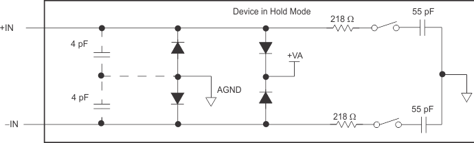 Figure 45. Input Equivalent Circuit
9.3.2 Power Saving
The device has an auto power-down feature. The device powers down at the end of every conversion. The input signal is acquired on sampling capacitors when the device is in power-down state. At the same time, the conversion results are available for reading. The device powers up automatically at the start of the conversion. The conversion runs on an internal clock and requires a fixed time. As a result, device power consumption is directly proportional to the speed of operation.
9.3.3 Digital Output
As discussed in the Description and Timing Diagrams sections, the device digital output is SPI-compatible. Table 1 lists the output codes corresponding to various analog input voltages.
Table 1. Output Codes
| DESCRIPTION | ANALOG VALUE (V) | DIGITAL OUTPUT STRAIGHT BINARY | |
|---|---|---|---|
| BINARY CODE | HEX CODE | ||
| Full-scale range | Vref | — | — |
| Least significant bit (LSB) | Vref / 65536 | — | — |
| Positive full-scale | +Vref – 1 LSB | 1111 1111 1111 1111 | FFFF |
| Mid-scale | Vref / 2 | 1000 0000 0000 0000 | 8000 |
| Mid-scale – 1 LSB | Vref / 2 – 1 LSB | 0111 1111 1111 1111 | 7FFF |
| Zero | 0 | 0000 0000 0000 0000 | 0000 |
9.3.4 SCLK Input
The device uses SCLK for the serial data output. Data are read after the conversion is complete and the device is in acquisition phase. A free-running SCLK can be used, but TI recommends stopping the clock during conversion time because the clock edges can couple with the internal analog circuit that, in turn, can affect the conversion results.
9.4 Device Functional Modes
The ADS8339 supports three interface options. Under each option, the device can be used with or without a busy indicator.
- CS mode for a 3-wire interface (with or without a busy indicator): This mode is useful for applications where a single ADS8339 device is connected to the digital host.
- CS mode for a 4-wire interface (with or without a busy indicator): This mode can be used when more than one ADS8339 device is connected to the digital host on a common data bus.
- Daisy-chain mode (with or without a busy indicator): This mode is provided to connect multiple ADS8339 devices in a chain (such as a shift register) and is useful when reducing the number of signal traces on the board or the component count.
The busy indicator is generated as the bit preceding the 16-bit serial data.
9.4.1 CS Mode for a 3-Wire Interface
CS mode is selected if SDI is high at the CONVST rising edge. As previously indicated, the device can be used without or with a busy indicator. This section discusses this interface and the two options in detail.
9.4.1.1 3-Wire CS Mode Without a Busy Indicator
In a 3-wire CS mode, SDI is permanently tied to +VBD, as shown in Figure 46. CONVST functions like CS. As shown in Figure 47, the device samples the input signal and enters the conversion phase on the CONVST rising edge. SDO goes to 3-state at the same time. Conversion is done with the internal clock and continues regardless of the state of CONVST. As a result, CONVST (functioning as CS) can be brought low after the start of the conversion to select other devices on the board.
CONVST must return to high before the minimum conversion time (tcnv_min in the Timing Requirements table) elapses. A high level on CONVST at the end of the conversion ensures the device does not generate a busy indicator.
 Figure 46. Connection Diagram: 3-Wire CS Mode without a Busy Indicator (SDI = 1)
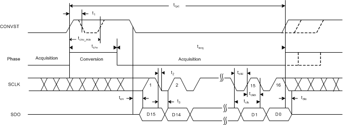 Figure 47. Interface Timing Diagram: 3-Wire CS Mode Without a Busy Indicator (SDI = 1)
When the conversion is complete, the device enters acquisition phase and powers down. On the CONVST falling edge, SDO comes out of 3-state and the device outputs the MSB of the data. Afterwards, the device outputs the next lower data bits on every subsequent SCLK falling edge. A minimum of 15 SCLK falling edges must occur during the low period of CONVST. SDO goes to 3-state after the 16th SCLK falling edge or when CONVST is high, whichever occurs first.
9.4.1.2 3-Wire CS Mode With a Busy Indicator
As stated in the 3-Wire CS Mode Without a Busy Indicator section, SDI is permanently tied to +VBD, as shown in Figure 48. CONVST functions like CS. As shown in Figure 49, the device samples the input signal and enters the conversion phase on the CONVST rising edge. SDO goes to 3-state at the same time. Conversion is done with the internal clock and continues regardless of the state of CONVST. As a result, CONVST (functioning as CS) can be toggled after the start of the conversion to select other devices on the board.
CONVST must return to low before the minimum conversion time (tcnv_min in the Timing Requirements table) elapses and remains low until the end of the maximum conversion time. A low level on the CONVST input at the end of a conversion ensures the device generates a busy indicator (low level on SDO). For fast settling, a 10-kΩ pull-up resistor tied to +VBD is recommended to provide the necessary current to drive SDO low.
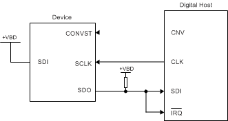 Figure 48. Connection Diagram: 3-Wire CS Mode With a Busy Indicator
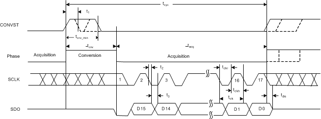 Figure 49. Interface Timing Diagram: 3-Wire CS Mode With a Busy Indicator (SDI = 1)
When the conversion is complete, the device enters acquisition phase, powers down, forces SDO out of 3-state, and outputs a busy indicator bit (low level). The device outputs the MSB of data on the first SCLK falling edge after the conversion is complete and continues to output the next lower data bits on every subsequent SCLK falling edge. A minimum of 16 SCLK falling edges must occur during the low period of CONVST. SDO goes to 3-state after the 17th SCLK falling edge or when CONVST is high, whichever occurs first.
9.4.2 CS Mode for a 4-Wire Interface
This interface is similar to the CS mode for 3-wire interface except that SDI is controlled by the digital host. This section discusses in detail the interface option with and without a busy indicator.
9.4.2.1 4-Wire CS Mode Without a Busy Indicator
As mentioned previously, in order to select CS mode, SDI must be high at the time of the CONVST rising edge. Unlike in the 3-wire interface option, SDI is controlled by the digital host and functions like CS. As shown in Figure 50, SDI goes to a high level before the CONVST rising edge. When SDI is high, the CONVST rising edge selects CS mode, forces SDO to 3-state, samples the input signal, and the device enters the conversion phase.
In the 4-wire interface option, CONVST must be at a high level from the start of the conversion until all data bits are read. Conversion is done with the internal clock and continues regardless of the state of SDI. As a result, SDI (functioning as CS) can be brought low to select other devices on the board.
SDI must return to high before the minimum conversion time (tcnv_min in the Timing Requirements table) elapses.
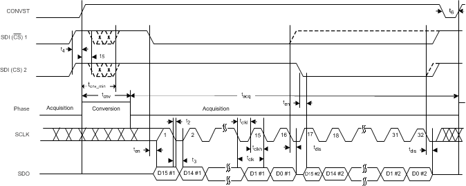 Figure 50. Interface Timing Diagram: 4-Wire CS Mode Without a Busy Indicator
When the conversion is complete, the device enters the acquisition phase and powers down. An SDI falling edge can occur after the maximum conversion time (tcnv in the Timing Requirements table). Note that SDI must be high at the end of the conversion so that the device does not generate a busy indicator. The SDI falling edge brings SDO out of 3-state and the device outputs the MSB of the data. Subsequently, the device outputs the next lower data bits on every subsequent SCLK falling edge. SDO goes to 3-state after the 16th SCLK falling edge or when SDI (CS) is high, whichever occurs first. As shown in Figure 51, multiple devices can be chained on the same data bus. In this case, the second device SDI (functioning as CS) can go low after the first device data are read and the device 1 SDO is in 3-state.
Care must be taken so that CONVST and SDI are not both low at any time during the cycle.
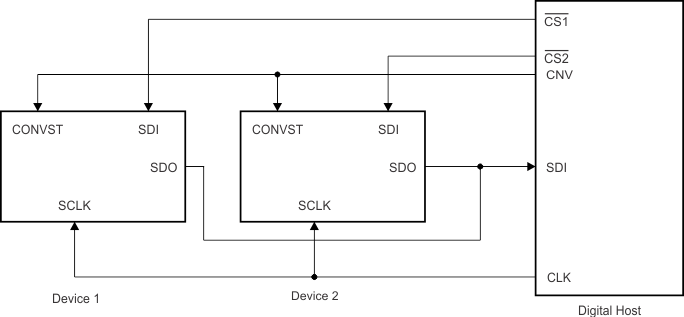 Figure 51. Connection Diagram: 4-Wire CS Mode Without a Busy Indicator
9.4.2.2 4-Wire CS Mode With a Busy Indicator
As mentioned previously, in order to select CS mode, SDI must be high at the time of the CONVST rising edge. In this mode of operation, the connection is made as shown in Figure 52.
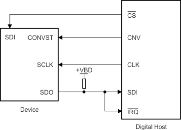 Figure 52. Connection Diagram: 4-Wire CS Mode With a Busy Indicator
Unlike in the 3-wire interface option, SDI is controlled by the digital host and functions like CS. As shown in Figure 53, SDI goes to a high level before the CONVST rising edge. When SDI is high, the CONVST rising edge selects the CS mode, forces SDO to 3-state, samples the input signal, and the device enters the conversion phase.
In the 4-wire interface option, CONVST must be at a high level from the start of the conversion until all data bits are read. Conversion is done with the internal clock and continues regardless of the state of SDI. As a result, SDI (functioning as CS) can be toggled to select other devices on the board.
SDI must return low before the minimum conversion time (tcnv_min in the Timing Requirements table) elapses and must remain low until the end of the maximum conversion time. A low level on the SDI input at the end of a conversion ensures the device generates a busy indicator (low on SDO). For fast settling, a 10-kΩ pull-up resistor tied to +VBD is recommended to provide the necessary current to drive SDO low.
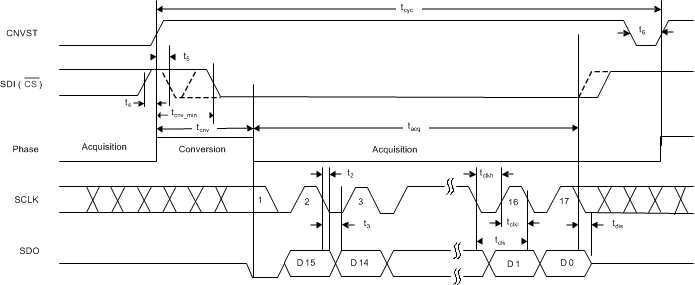 Figure 53. Interface Timing Diagram: 4-Wire CS Mode With a Busy Indicator
When the conversion is complete, the device enters acquisition phase, powers down, forces SDO out of 3-state, and outputs a busy indicator bit (low level). The device outputs the MSB of the data on the first SCLK falling edge after the conversion is complete and continues to output the next lower data bits on every subsequent SCLK falling edge. SDO goes to 3-state after the 17th SCLK falling edge or when SDI (CS) is high, whichever occurs first.
Care must be taken so that CONVST and SDI are not both low at any time during the cycle.
9.4.3 Daisy-Chain Mode
Daisy-chain mode is selected if SDI is low at the time of the CONVST rising edge. This mode is useful to reduce wiring and hardware requirements (such as digital isolators in applications where multiple ADC devices are used). In this mode, all devices are connected in a chain (the SDO of one device is connected to the SDI of the next device) and data transfer is analogous to a shift register.
As in CS mode, this mode offers operation with or without a busy indicator. This section discusses these interface options in detail.
9.4.3.1 Daisy-Chain Mode Without a Busy Indicator
A connection diagram for this mode is shown in Figure 54. The SDI for device 1 is tied to ground and the SDO of device 1 goes to the SDI of device 2, and so on. The SDO of the last device in the chain goes to the digital host. CONVST for all devices in the chain are tied together. There is no CS signal in this mode.
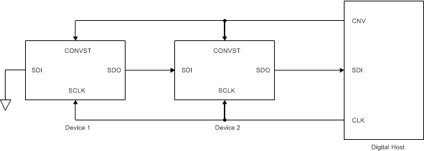 Figure 54. Connection Diagram: Daisy-Chain Mode Without a Busy Indicator (SDI = 0)
The device SDO is driven low when SDI low selects daisy-chain mode and the device samples the analog input and enters the conversion phase. SCLK must be low at the CONVST rising edge (as shown in Figure 55) so that the device does not generate a busy indicator at the end of the conversion. In this mode, CONVST remains high from the start of the conversion until all data bits are read. When started, the conversion continues regardless of the state of SCLK.
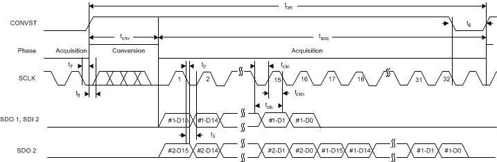 Figure 55. Interface Timing Diagram: Daisy-Chain Mode Without a Busy Indicator
At the end of the conversion, every device in the chain initiates an output of its conversion data starting with the MSB bit. Furthermore, the next lower data bit is output on every subsequent SCLK falling edge. While every device outputs its data on the SDO pin, each device also receives the previous device data on the SDI pin (other than device 1) and stores the data in the shift register. The device latches incoming data on every SCLK falling edge. The SDO of the first device in the chain goes low after the 16th SCLK falling edge. All subsequent devices in the chain output the stored data from the previous device in MSB-first format immediately following their own data word. 16 × N clocks must read data for N devices in the chain.
9.4.3.2 Daisy-Chain Mode With a Busy Indicator
A connection diagram for this mode is shown in Figure 56. The SDI for device 1 is wired to its CONVST and the CONVST for all devices in the chain are wired together. The SDO of device 1 goes to the SDI of device 2, and so on. The SDO of the last device in the chain goes to the digital host. There is no CS signal in this mode.
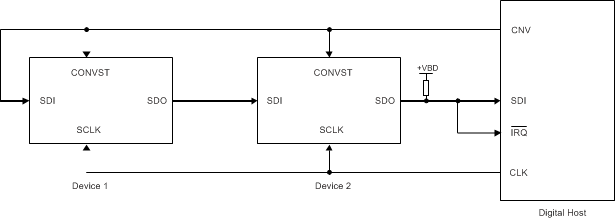 Figure 56. Connection Diagram: Daisy Chain Mode With a Busy Indicator (SDI = 0)
On the CONVST rising edge, all devices in the chain sample the analog input and enter the conversion phase. For the first device, SDI and CONVST are wired together and the setup time of SDI to the CONVST rising edge is adjusted so that the device still enters daisy-chain mode even though SDI and CONVST rise together. SCLK must be high at the CONVST rising edge (as shown in Figure 57) so that the device generates a busy indicator at the end of the conversion. In this mode, CONVST remains high from the start of the conversion until all data bits are read. When started, the conversion continues regardless of the state of SCLK.
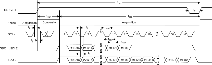 Figure 57. Interface Timing Diagram: Daisy Chain Mode With a Busy Indicator
At the end of the conversion, all devices in the chain generate busy indicators. On the first SCLK falling edge following the busy indicator bit, all devices in the chain output their conversion data starting with the MSB bit. Afterwards, the next lower data bit is output on every SCLK falling edge. While every device outputs its data on the SDO pin, each device also receives the previous device data on the SDI pin (except for device 1) and stores the data in the shift register. Each device latches incoming data on every SCLK falling edge. The SDO of the first device in the chain goes high after the 17th SCLK falling edge. All subsequent devices in the chain output the stored data from the pervious device in MSB-first format immediately following their own data word. 16 × N + 1 clock pulses are required to read data for N devices in the chain.