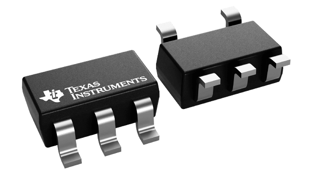
封装信息
| 封装 | 引脚 SOT-23 (DBV) | 5 |
| 工作温度范围 (°C) -40 to 125 |
| 包装数量 | 包装 250 | SMALL T&R |
SN74LVC1G86 的特性
- 符合从 –40°C 到 +125°C 的要求
- 支持 5V VCC 运行
- 输入端具有过压容限,最高可达 5.5V
- 支持向下转换到 VCC
- 在 3.3V 和 15pF 负载条件下,最大 tpd 为 4ns
- 低功耗,85°C 时 ICC 最大值为 10µA
- 3.3V 时,输出驱动为 ±24mA
- Ioff 支持局部关断模式和后驱动保护
- 采用德州仪器 (TI) NanoFree™ 封装
- 闩锁性能超过 100mA,符合 JESD 78 II 类规范的要求
SN74LVC1G86 的说明
SN74LVC1G86 器件以正逻辑执行布尔函数 Y = AB + A B。该单路 2 输入异或门专为在 1.65V 至 5.5V VCC 电压下运行而设计。
如果输入为低电平,则可在输出时重新生成真实形态的其他输入。如果输入为高电平,另一个输入的信号则可在输出时重新生成反向信号。该器件具有低功耗,在 3.3V 和 15pF 容性负载条件下,tpd 最大值为 4ns。最大输出驱动为 ±32mA(4.5V 时)和 ±24mA(3.3V 时)。
该器件专用于使用 Ioff 的局部断电应用。Ioff 电路可禁用输出,以防在器件断电时破坏性电流通过该器件回流。