ZHCU741 July 2020
- 说明
- 资源
- 特性
- 应用
- 5
- 1System Description
- 2System Overview
-
3Hardware, Software, Testing Requirements, and Test Results
- 3.1 Hardware Requirements
- 3.2 Test Setup
- 3.3
Test Results
- 3.3.1 Boost Turn on Delay
- 3.3.2 Highbeam/Lowbeam Turn on Delay
- 3.3.3 Highbeam/Lowbeam Switch Node and Ripple Current
- 3.3.4 Turn Indicator Turn on Delay
- 3.3.5 Turn Indictor Turn Off Delay
- 3.3.6 Turn Indicator 1.5 Hz Operation
- 3.3.7 Turn Indicator Output Voltage and Current
- 3.3.8 Daytime Running Light Turn-on Delay
- 3.3.9 Daytime Running Light Switch Node and Output Current
- 3.3.10 Highbeam/Lowbeam LED Short
- 3.3.11 Highbeam/Lowbeam Fault Indicator
- 3.3.12 Turn Indicator Fault Output
- 3.3.13 TPS92682-Q1 Boost and SEPIC Interleaving
- 3.3.14 TIDA-050040 Full Load Efficiency
- 3.3.15 Efficiency Highbeam/Lowbeam
- 3.3.16 Efficiency Turn Indicator and Daytime Running Light
- 3.3.17 Efficiency Highbeam/Lowbeam and Turn Indicator
- 3.3.18 CISPR 25 Class 5 EMI Scan
- 3.3.19 Top Side Thermal Image DRL at 15W
- 3.3.20 Bottom side thermal image DRL at 15W
- 3.3.21 Top Side Thermal Image Highbeam/Lowbeam at 30W, Turn Indicator at 7.5W average
- 3.3.22 Bottom Side Thermal Image Highbeam/Lowbeam at 30W, Turn Indicator at 7.5W average
- 4Design and Documentation Support
2.3.5 System Design Theory
The input power connects to EC1, the edge card connector, as three power inputs. Lowbeam power is fed to reverse protection diodes D19 and D20. 1.5 Hz Turn Indicator power is fed to reverse protection diode D12. Daytime Running Light/Position Marker Light power input is fed to reverse protection diode D18. A P-channel MOSFET, Q6, is across D18 to reduce Lowbeam input current to zero when there is a Highbeam/Lowbeam fault. All power lines are signal detected and sent to the microprocessor, U10. An additional input signal, Highbeam, is reverse diode protected and sent to the microprocessor. Highbeam is powered from the Lowbeam power input. HB_LED output is the drain of Q9 used to shunt the Highbeam portion of the Highbeam/Lowbeam LED string. All input power lines after the reverse protection diodes are tied together and sent to an EMI filter. The output of the EMI filter provides power to the TPS92682-Q1, channel one a Constant Voltage boost, channel two a Constant Current SEPIC converter. The Constant Voltage Boost feeds the TPS92520-Q1 dual buck converter for Highbeam/Lowbeam and Turn Indicator. A detailed design procedure can be found in the TPS92682-Q1 data sheet and TPS92520-Q1 data sheet.
Constant Voltage boost converter calculations:
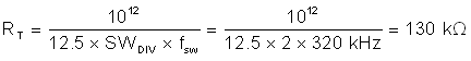
The Calculation for the timing resistor for 320 KHz switching frequency is:
where
• SWDIV is 2. This is the default division factor in SWDIV register 03h of the TPS92682-Q1 device.
• fSW is the switching frequency of the circuit. A value of 130 kΩ is selected for R31.
Calculating Boost output power assuming a worst case buck converter efficiency of 90%: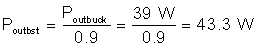
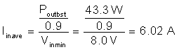
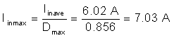
The first step to calculate the cycle by cycle current limit resistor value is to calculate average maximum input current:
where
• Vinmin is the minimum input voltage at maximum output power, 8.0V is used
• 0.9 is used for worst case Boost converter efficiency
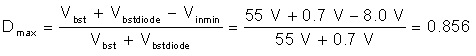
The next step is to calculate the duty cycle at maximum input current:
where
• Vbst is the boost output voltage
• Vbstdiode is the forward voltage of the boost diode, 0.7V is used
• Vinmin is the minimum voltage for maximum output power, 8.0V is used
Using the duty cycle the maximum average on-time input current can be calculated:
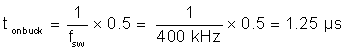
To calculate peak current the peak to peak current ripple at maximum output power needs to be calculated, the first step is calculating ton:
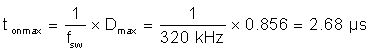
where
• fsw is the switching frequency, 320 kHz
The peak to peak inductor ripple can be calculated using the previous calculations:
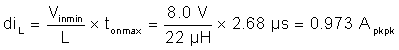
where
• L is the inductor value, 22 μH is chosen for this design
By summing the maximum average on-time current and half of the peak to peak current ripple the peak current can be calculated:
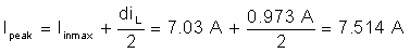
The maximum peak current can now be used to calculate the Ris resistor value
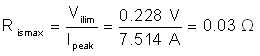
where
• Vilim is the TPS92682-Q1 minimum peak current trip threshold when CHxILIM = 11, register 0x0E
The design uses two 0.04 ohm resistors in parallel for margin and testing.
Calculations for the TPS92520-Q1:
The two TPS92520-Q1 synchronous buck converters are set up with the same components and same operational range. The switching frequencies of the buck converters are 384 kHz for Lowbeam/Highbeam and 438 kHz for Turn Indicator set by registers 0x11 and 0x12.
Maximum current ripple occurs when Vled is half of the input voltage, using 400 kHz for the on-time and 50% duty cycle:
Peak to peak current ripple can be calculated using tonbuck along with the inductor value and Vled at half of Vbst, 55V:
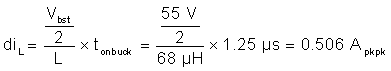
where
• L is the inductor value, 68 μH is chosen for this design
• fsw is set to 400 kHz
Maximum output current for both channels using Rcs value:
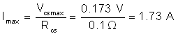
where
• Vcsmax is 0.173V from the TPS92520-Q1 datasheet current sense threshold
• Rcs is the current sense resistor, 0.1Ω is chosen