ZHCU741 July 2020
- 说明
- 资源
- 特性
- 应用
- 5
- 1System Description
- 2System Overview
-
3Hardware, Software, Testing Requirements, and Test Results
- 3.1 Hardware Requirements
- 3.2 Test Setup
- 3.3
Test Results
- 3.3.1 Boost Turn on Delay
- 3.3.2 Highbeam/Lowbeam Turn on Delay
- 3.3.3 Highbeam/Lowbeam Switch Node and Ripple Current
- 3.3.4 Turn Indicator Turn on Delay
- 3.3.5 Turn Indictor Turn Off Delay
- 3.3.6 Turn Indicator 1.5 Hz Operation
- 3.3.7 Turn Indicator Output Voltage and Current
- 3.3.8 Daytime Running Light Turn-on Delay
- 3.3.9 Daytime Running Light Switch Node and Output Current
- 3.3.10 Highbeam/Lowbeam LED Short
- 3.3.11 Highbeam/Lowbeam Fault Indicator
- 3.3.12 Turn Indicator Fault Output
- 3.3.13 TPS92682-Q1 Boost and SEPIC Interleaving
- 3.3.14 TIDA-050040 Full Load Efficiency
- 3.3.15 Efficiency Highbeam/Lowbeam
- 3.3.16 Efficiency Turn Indicator and Daytime Running Light
- 3.3.17 Efficiency Highbeam/Lowbeam and Turn Indicator
- 3.3.18 CISPR 25 Class 5 EMI Scan
- 3.3.19 Top Side Thermal Image DRL at 15W
- 3.3.20 Bottom side thermal image DRL at 15W
- 3.3.21 Top Side Thermal Image Highbeam/Lowbeam at 30W, Turn Indicator at 7.5W average
- 3.3.22 Bottom Side Thermal Image Highbeam/Lowbeam at 30W, Turn Indicator at 7.5W average
- 4Design and Documentation Support
3.1 Hardware Requirements
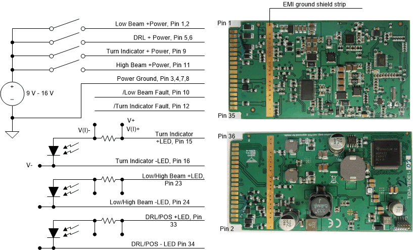
 Figure 3-1 TIDA-50040 Test Connections
for efficiency measurements, turn-on, turn-off delays and steady state
operation. Test setup showing switched inputs, outputs, PCB edge connector pin numbers
and connections for measurements.
Figure 3-1 TIDA-50040 Test Connections
for efficiency measurements, turn-on, turn-off delays and steady state
operation. Test setup showing switched inputs, outputs, PCB edge connector pin numbers
and connections for measurements.A 0 V to 25 V, 10A minimum DC lab supply is required for maximum power testing and efficiency measurements. For testing a Hewlett Packard 6010A DC supply provides power to the test board. Custom software is loaded to allow full output power from each stage when powered from their respective inputs. Four volt meters measure input voltage and current as well as each channel's output voltage and current. Input current is measured through a current shunt, output currents are measured across a 0.1 Ω precision resistor. A tektronics TDS5054B displayed oscilloscope measurements for voltage and current waveforms. To run maximum output power a custom LED load board was developed. A function generator set to 1.5 Hz 0 V to 5 V drives the Turn Indicator input for delay measurements.
The Turn Indicator LED load to operate with single LED fault detection needs to fall within 6.9 V to 7.7 V at 40 mA using four amber LEDs. The LED load for Lowbeam needs to fall within 10 V to 11.2 V at 70 mA using four white LEDs. The LED load for Highbeam needs to fall within 20.2 V to 22.4 V using eight LEDs, four for Lowbeam in series with four for Highbeam. The center of the string ties to HB_LED to allow shunt of the Highbeam portion of the LED string. The RBIN resistor to ground value for Lowbeam is 20 kΩ. The RBIN resistors for Turn Indicator and Daytime Running Light are 30 kΩ.
PIN NUMBER | PIN NAME | PIN DESCRIPTION | PIN NUMBER | PIN NAME | PIN DESCRIPTION |
|---|---|---|---|---|---|
1 | LB1 | Power Input for LB and HB | 2 | LB2 | Power Input for LB and HB |
3 | Power GND | Input Power Ground | 4 | Power GND | Input Power Ground |
5 | DRLPOS1 | Power input for DRL/POS | 6 | DRLPOS2 | Input Power for DRL/POS |
7 | Power GND | Input Power Ground | 8 | Power Ground | Input Power Ground |
9 | TI | Power Input for TI | 10 | LB_Fault | Open Collector HB/LB Fault |
11 | HB | Signal Input for HB shunt MOSFET | 12 | TI_Fault | Open Collector TI Fault |
13 | NC | 14 | NC | ||
15 | DRLPOS+ | DRL/POS +LED Connection | 16 | Power GND | DRL/POS -LED Connection |
17 | NC | 18 | DRLPOS_RBIN | DRL/POS Binning Resistor Input | |
19 | Signal GND | Return for RBIN and NTC | 20 | DRLPOS_NTC | DRL/POS Thermal Feedback |
21 | NC | 22 | NC | ||
23 | LBHB+ | LB/HB +LED Connection | 24 | Power GND | LB/HB -LED Connection |
25 | HB_LED | HB Shunt Output | 26 | LBHB_RBIN | LB/HB Binning Resistor |
27 | Signal GND | Return for RBIN and NTC | 28 | LBHB_NTC | LB/HB Thermal Feedback |
29 | NC | 30 | NC | ||
31 | NC | 32 | Power GND | TI -LED Connection | |
33 | TI+ | TI +LED Connection | 34 | TI_RBIN | TI Binning Resistor |
35 | Signal GND | Return for RVIN and NTC | 36 | TI_NTC | TI Thermal Feedback |