ZHCSLD2E may 2020 – july 2023 UCC28782
PRODUCTION DATA
- 1
- 1 特性
- 2 应用
- 3 描述
- 4 Revision History
- 5 Device Comparison Table
- 6 Pin Configuration and Functions
- 7 Specifications
-
8 Detailed Description
- 8.1 Overview
- 8.2 Functional Block Diagram
- 8.3
Detailed Pin Description
- 8.3.1 BUR Pin (Programmable Burst Mode)
- 8.3.2 FB Pin (Feedback Pin)
- 8.3.3 REF Pin (Internal 5-V Bias)
- 8.3.4 VDD Pin (Device Bias Supply)
- 8.3.5 P13 and SWS Pins
- 8.3.6 S13 Pin
- 8.3.7 IPC Pin (Intelligent Power Control Pin)
- 8.3.8 RUN Pin (Driver and Bias Source for Isolator)
- 8.3.9 PWMH and AGND Pins
- 8.3.10 PWML and PGND Pins
- 8.3.11 SET Pin
- 8.3.12 RTZ Pin (Sets Delay for Transition Time to Zero)
- 8.3.13 RDM Pin (Sets Synthesized Demagnetization Time for ZVS Tuning)
- 8.3.14 BIN, BSW, and BGND Pins
- 8.3.15 XCD Pin
- 8.3.16 CS, VS, and FLT Pins
- 8.4
Device Functional Modes
- 8.4.1 Adaptive ZVS Control with Auto-Tuning
- 8.4.2 Dead-Time Optimization
- 8.4.3 EMI Dither and Dither Fading Function
- 8.4.4 Control Law across Entire Load Range
- 8.4.5 Adaptive Amplitude Modulation (AAM)
- 8.4.6 Adaptive Burst Mode (ABM)
- 8.4.7 Low Power Mode (LPM)
- 8.4.8 First Standby Power Mode (SBP1)
- 8.4.9 Second Standby Power Mode (SBP2)
- 8.4.10 Startup Sequence
- 8.4.11 Survival Mode of VDD (INT_STOP)
- 8.4.12 Capacitor Voltage Balancing Function
- 8.4.13 Device Functional Modes for Bias Regulator Control
- 8.4.14
System Fault Protections
- 8.4.14.1 Brown-In and Brown-Out
- 8.4.14.2 Output Over-Voltage Protection (OVP)
- 8.4.14.3 Input Over Voltage Protection (IOVP)
- 8.4.14.4 Over-Temperature Protection (OTP) on FLT Pin
- 8.4.14.5 Over-Temperature Protection (OTP) on CS Pin
- 8.4.14.6 Programmable Over-Power Protection (OPP)
- 8.4.14.7 Peak Power Limit (PPL)
- 8.4.14.8 Output Short-Circuit Protection (SCP)
- 8.4.14.9 Over-Current Protection (OCP)
- 8.4.14.10 External Shutdown
- 8.4.14.11 Internal Thermal Shutdown
- 8.4.15 Pin Open/Short Protections
-
9 Application and Implementation
- 9.1 Application Information
- 9.2
Typical Application Circuit
- 9.2.1 Design Requirements for a 65-W USB-PD Adapter Application
- 9.2.2
Detailed Design Procedure
- 9.2.2.1 Input Bulk Capacitance and Minimum Bulk Voltage
- 9.2.2.2 Transformer Calculations
- 9.2.2.3 Clamp Capacitor Calculation
- 9.2.2.4 Bleed-Resistor Calculation
- 9.2.2.5 Output Filter Calculation
- 9.2.2.6 Calculation of ZVS Sensing Network
- 9.2.2.7 Calculation of BUR Pin Resistances
- 9.2.2.8 Calculation of Compensation Network
- 9.2.3 Application Curves
- 10Power Supply Recommendations
- 11Layout
- 12Device and Documentation Support
- 13Mechanical, Packaging, and Orderable Information
8.3.4 VDD Pin (Device Bias Supply)
The VDD pin is the primary bias for the internal 5-V REF regulator, internal 13-V P13 regulator, other internal references, and the undervoltage lock-out (UVLO) circuit. As shown in Figure 8-5, the UVLO circuit connected to the VDD pin controls the internal power-path switches among VDD, P13, and SWS pins, in order to allow an external depletion-mode MOSFET (QS) to be able to perform both VVDD startup and switch-node voltage (VSW) sensing for ZVS control after startup. During startup, SWS and P13 pins are connected to VDD pin allowing QS to charge the VDD capacitor (CVDD) from the VSW. After VDD startup completes, the ZVS discriminator block and switching logic are enabled. Then, the transformer starts delivering energy to the output capacitor (CO) every switching cycle, so both output voltage (VO) and auxiliary winding voltage (VAUX) increase. As VAUX is high enough, the auxiliary winding will take over to power VVDD. The UVLO circuit provides a turn-on threshold of VVDD(ON) at 17 V and turn-off threshold of VVDD(OFF) at 10.6 V. For fixed output voltage ACF converter designs, the wide VVDD range can accommodate lower values of VDD capacitor (CVDD) and support shorter power-on delays. For ACF designs requiring wide output voltage range, the integrated switching regulator converts the rectified VAUX to an 18.5-V regulation level of VVDD. Compared with the conventional bias approach with a high-voltage linear regulator and multiple auxiliary windings, the footprint and conversion efficiency of the integrated switching regulator are improved greatly. For a wide-output design using the bias regulator, a 10 to 15-µF ceramic VDD capacitor is recommended to hold up VVDD during soft start and to provide decoupling for the regulator switching loop. Section 8.4.10 of this datasheet describes the details on the startup sequencing with the switching regulator.
For a fixed output voltage design, both the BIN and BSW pins should be shorted to BGND, and the rectified VAUX is directly connected to the VDD pin. As VVDD reaches VVDD(ON), the SWS pin is disconnected from the VDD pin by the internal power path switch, so the CVDD size has to be sufficient to hold VVDD higher than VVDD(OFF) until the positive auxiliary winding voltage is high enough to take over bias power delivery during VO soft start. Therefore, the calculation of minimum capacitance (CVDD(MIN)) needs to consider the discharging effect from the sink current of the UCC28782 during switching in its run state (IRUN(SW)), the average operating current of driver (IDR), and the average gate charge current of half-bridge FETs (IQg) throughout the longest time of VO soft start (tSS(MAX)).
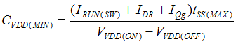
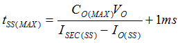
tSS(MAX) estimation should consider the averaged soft-start current (ISEC(SS)) on the secondary side of ACF, the constant-current output load (IO(SS)) (if any), maximum output capacitance (CO(MAX)), and a 0.7-ms time-out potentially being triggered in the startup sequence. 1 ms is applied in the equation to be the worst-case condition of the 0.7-ms timer.
During VO soft start, VCST reaches the maximum current threshold on the CS pin (VCST(MAX)) , so ISEC(SS) at the minimum voltage of the input bulk capacitor (VBULK(MIN)) can be approximated as:
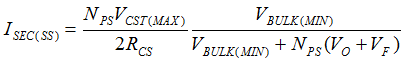
where RCS is the current sense resistor, NPS is primary-to-secondary turns ratio, and VF is the forward voltage drop of the secondary rectifier.