ZHCSLD2E may 2020 – july 2023 UCC28782
PRODUCTION DATA
- 1
- 1 特性
- 2 应用
- 3 描述
- 4 Revision History
- 5 Device Comparison Table
- 6 Pin Configuration and Functions
- 7 Specifications
-
8 Detailed Description
- 8.1 Overview
- 8.2 Functional Block Diagram
- 8.3
Detailed Pin Description
- 8.3.1 BUR Pin (Programmable Burst Mode)
- 8.3.2 FB Pin (Feedback Pin)
- 8.3.3 REF Pin (Internal 5-V Bias)
- 8.3.4 VDD Pin (Device Bias Supply)
- 8.3.5 P13 and SWS Pins
- 8.3.6 S13 Pin
- 8.3.7 IPC Pin (Intelligent Power Control Pin)
- 8.3.8 RUN Pin (Driver and Bias Source for Isolator)
- 8.3.9 PWMH and AGND Pins
- 8.3.10 PWML and PGND Pins
- 8.3.11 SET Pin
- 8.3.12 RTZ Pin (Sets Delay for Transition Time to Zero)
- 8.3.13 RDM Pin (Sets Synthesized Demagnetization Time for ZVS Tuning)
- 8.3.14 BIN, BSW, and BGND Pins
- 8.3.15 XCD Pin
- 8.3.16 CS, VS, and FLT Pins
- 8.4
Device Functional Modes
- 8.4.1 Adaptive ZVS Control with Auto-Tuning
- 8.4.2 Dead-Time Optimization
- 8.4.3 EMI Dither and Dither Fading Function
- 8.4.4 Control Law across Entire Load Range
- 8.4.5 Adaptive Amplitude Modulation (AAM)
- 8.4.6 Adaptive Burst Mode (ABM)
- 8.4.7 Low Power Mode (LPM)
- 8.4.8 First Standby Power Mode (SBP1)
- 8.4.9 Second Standby Power Mode (SBP2)
- 8.4.10 Startup Sequence
- 8.4.11 Survival Mode of VDD (INT_STOP)
- 8.4.12 Capacitor Voltage Balancing Function
- 8.4.13 Device Functional Modes for Bias Regulator Control
- 8.4.14
System Fault Protections
- 8.4.14.1 Brown-In and Brown-Out
- 8.4.14.2 Output Over-Voltage Protection (OVP)
- 8.4.14.3 Input Over Voltage Protection (IOVP)
- 8.4.14.4 Over-Temperature Protection (OTP) on FLT Pin
- 8.4.14.5 Over-Temperature Protection (OTP) on CS Pin
- 8.4.14.6 Programmable Over-Power Protection (OPP)
- 8.4.14.7 Peak Power Limit (PPL)
- 8.4.14.8 Output Short-Circuit Protection (SCP)
- 8.4.14.9 Over-Current Protection (OCP)
- 8.4.14.10 External Shutdown
- 8.4.14.11 Internal Thermal Shutdown
- 8.4.15 Pin Open/Short Protections
-
9 Application and Implementation
- 9.1 Application Information
- 9.2
Typical Application Circuit
- 9.2.1 Design Requirements for a 65-W USB-PD Adapter Application
- 9.2.2
Detailed Design Procedure
- 9.2.2.1 Input Bulk Capacitance and Minimum Bulk Voltage
- 9.2.2.2 Transformer Calculations
- 9.2.2.3 Clamp Capacitor Calculation
- 9.2.2.4 Bleed-Resistor Calculation
- 9.2.2.5 Output Filter Calculation
- 9.2.2.6 Calculation of ZVS Sensing Network
- 9.2.2.7 Calculation of BUR Pin Resistances
- 9.2.2.8 Calculation of Compensation Network
- 9.2.3 Application Curves
- 10Power Supply Recommendations
- 11Layout
- 12Device and Documentation Support
- 13Mechanical, Packaging, and Orderable Information
8.4.6 Adaptive Burst Mode (ABM)
As the load current reduces to IO(BUR) where VCS reaches the VCST(BUR) threshold, the control mode transitions to ABM starts and VCS is clamped. The peak magnetizing current and the switching frequency (fSW) of each switching cycle are fixed for a given input voltage level. VCST(BUR) is programmed by the BUR pin voltage (VBUR). The PWM pattern of ABM is shown in Figure 8-27. When RUN goes high, a delay time between RUN and PWML (tD(RUN-PWML)) is given to allow both the gate driver and the UCC28782 time to wake up from a wait state to a run state. PWML is set as the first pulse to build up the bootstrap voltage of the high-side driver before PWMH starts switching. The first PWML pulse turns on QL close to a valley point of the DCM ringing on the switch-node voltage (VSW) by sensing the condition of zero crossing detection (ZCD) on the auxiliary winding voltage (VAUX). The following switching cycles operate in a ZVS condition, since PWMH is enabled. As the number of PWML pulses (NSW) in the burst packet reaches its target value, the RUN pin pulls low after the ZCD of the last switching cycle is detected, and forces the half-bridge driver and UCC28782 into a wait state for the quiescent current reduction of both devices. In this mode, the minimum off-time of the RUN signal is 2.2 µs and the minimum on-time of PWML is limited to the leading-edge blanking time (tCSLEB) of the peak current loop. However, more grouped pulses means more risk of higher output ripple and higher audible noise. The following equation estimates how burst frequency (fBUR) varies with output load and other parameters.
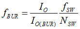
As IO < IO(BUR), fBUR can become lower than the audible noise range if NSW is fixed. In ABM, NSW is modulated to ensure fBUR stays above 20 kHz by monitoring fBUR in each burst period. As IO reduces, fBUR becomes lower and reaches a predetermined low-level frequency threshold (fBUR(LR)) of 25 kHz. The ABM loop commands Nsw of both PWML and PWMH to be reduced by one pulse to maintain fBUR above fBUR(LR). At the same time, the burst frequency ripple on the output voltage reduces as NSW drops with the load reduction. As IO increases, fBUR becomes higher and reaches a predetermined high-level frequency threshold (fBUR(UP)). The ABM loop commands NSW to be increased by one pulse to push fBUR back below fBUR(UP).
The maximum NSW and the fBUR(UP) thresholds are modified based on the output voltage condition, i.e., the positive VS-pin voltage level. When the VVS sampled at the PWMH falling edge is less than the 2.4-V threshold (VVSLV(LR)), the maximum NSW is 5 pulses and the fBUR(UP2) is 50 kHz. When the sampled VVS is higher than the 2.5-V threshold (VVSLV(UP)), the maximum NSW is 9 pulses, the fBUR(UP2) is 50 kHz for NSW ≤ 3, and the fBUR(UP1) is 34 kHz for NSW> 3. The IPC-pin voltage does not affect the parameters in ABM mode.
This algorithm maximizes the number of pulses in each burst packet to improve light-load efficiency, while also limiting the burst output ripple and audible noise. As IO is close to the boundary between AAM and ABM, the two burst packets with the maximum pulse count may start to bundle together. In order to mitigate the output ripple and audible noise concerns, when the bundled burst packet appears two times within eight sequential burst cycles, the 5-µA current sink into the BUR pin is enabled to reduce VBUR . The less energy per cycle with a lower VBURwill force the control loop to transition from ABM to AAM smoothly in order to allow the peak current increase to maintain the output voltage regulation.
 Figure 8-27 PWM Pattern in ABM