ZHCSHM2D June 2018 – April 2025 TPS746-Q1
PRODUCTION DATA
- 1
- 1 特性
- 2 应用
- 3 说明
- 4 Pin Configuration and Functions
- 5 Specifications
- 6 Detailed Description
- 7 Application and Implementation
- 8 Device and Documentation Support
- 9 Revision History
- 10Mechanical, Packaging, and Orderable Information
7.2.2.1 Input Current
During normal operation, the input current to the LDO is approximately equal to the output current of the LDO. During startup, the input current is higher as a result of the inrush current charging the output capacitor. Use Equation 6 to calculate the current through the input.
Equation 6. 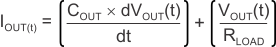
where:
- VOUT(t) is the instantaneous output voltage of the turn-on ramp
- dVOUT(t) / dt is the slope of the VOUT ramp
- RLOAD is the resistive load impedance