ZHCS987C June 2012 – September 2017
PRODUCTION DATA.
- 1 特性
- 2 应用
- 3 说明
- 4 修订历史
- 5 Pin Configuration and Functions
-
6 Specifications
- 6.1 Absolute Maximum Ratings
- 6.2 ESD Ratings
- 6.3 Recommended Operating Conditions
- 6.4 Thermal Information
- 6.5 Electrical Characteristics: Front-End Amplification (Weight-Scale Signal Chain)
- 6.6 Electrical Characteristics: Body Composition Measurement Front-End
- 6.7 Electrical Characteristics: Analog-to-Digital Converter
- 6.8 Electrical Characteristics: Digital Input/Output
- 6.9 Timing Requirements: Serial Interface Timing
- 6.10 Typical Characteristics
-
7 Detailed Description
- 7.1 Overview
- 7.2 Functional Block Diagram
- 7.3 Feature Description
- 7.4 Device Functional Modes
- 7.5 Programming
- 7.6
Register Maps
- 7.6.1
Register Map
- 7.6.1.1 ADC_DATA_RESULT (Address 0x00, Default 0x0000)
- 7.6.1.2 ADC_CONTROL_REGISTER1 (Address 0x01, Default 0x01C3)
- 7.6.1.3 MISC_REGISTER1 (Address 0x02, Default 0x8000)
- 7.6.1.4 MISC_REGISTER2 (Address 0x03, Default 0x7FFF)
- 7.6.1.5 DEVICE_CONTROL1 (Address 0x09, Default 0x0000)
- 7.6.1.6 ISW_MUX (Address 0x0A, Default 0x0000)
- 7.6.1.7 VSENSE_MUX (Address 0x0B, Default 0x0000)
- 7.6.1.8 IQ_MODE_ENABLE (Address 0x0C, Default 0x0000)
- 7.6.1.9 WEIGHT_SCALE_CONTROL (Address 0x0D, Default 0x0000)
- 7.6.1.10 BCM_DAC_FREQ (Address 0x0E, Default 0x0000)
- 7.6.1.11 DEVICE_CONTROL2 (Address 0x0F, Default 0x0000)
- 7.6.1.12 ADC_CONTROL_REGISTER2 (Address 0x10, Default 0x0000)
- 7.6.1.13 MISC_REGISTER3 (Address 0x1A, Default 0x0000)
- 7.6.1
Register Map
- 8 Application and Implementation
- 9 Power Supply Recommendations
- 10Layout
- 11器件和文档支持
- 12机械、封装和可订购信息
8 Application and Implementation
NOTE
Information in the following applications sections is not part of the TI component specification, and TI does not warrant its accuracy or completeness. TI’s customers are responsible for determining suitability of components for their purposes. Customers should validate and test their design implementation to confirm system functionality.
8.1 Application Information
8.1.1 BCM Channel Connections
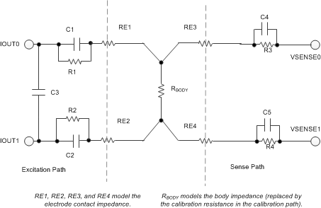
The suggested connections of the BCM excitation and sense electrodes to the device pins are shown in Figure 12. The circuit shows an electrical model of the body impedance being measured (RBODY) along with models for the electrode contact impedances. The components connecting the electrodes to the IOUTx and VSENSEx pins are meant to be replicated in the path of the calibration impedances as well. Suggestions for the component values are shown in Table 4.
 Figure 12. Connection of BCM Pins to Electrodes
Table 4. Component Values Corresponding to Figure 12(1)
8.1.2 Handling Oscillation of the Excitation Amplifier
The phase margin of the excitation amplifier can degrade if there is high capacitance at the input and output terminals. High capacitances can result can result from the capacitances from the electrodes, from protection diodes (for instance, ESD diodes), as well as the capacitance presented by the human body. Degradation of phase margin resulting from high capacitances can result in oscillations leading to reduced measurement accuracy. One way to improve the phase margin of the excitation amplifier is to introduce a series R-C at the output of the excitation amplifier in every measurement. This process is done using the components RCM = 1 kΩ and CCM = 1 nF in the simplistic model shown in Figure 13. This illustration is for a case where IOUT0 and IOUT1 are switched to the input and output of the excitation amplifier, respectively.
 Figure 13. Oscillation Fix of the Excitation Amplifier
Such a scheme can be implemented in one of two methods:
- A separate RCM-CCM for every IOUTx and RPx pin that gets switched to the excitation amplifier output.
- A single RCM-CCM on one of the RPx pins that gets switched to the excitation amplifier output during calibration. When not using this RPx pin, still switch the same RPx pin to the output of the excitation amplifier (in addition to whichever other pin is switched to the output) so that the RCM-CCM still gets connected to the output of the excitation amplifier.
Method 2 is preferable because this method involves only one RCM and one CCM.
8.1.3 Achieving Deterministic Phase in the IQ Mode
The DAC frequency generator (DDS) is initialized on the register update of the DAC frequency register. The IQ demod clock divider is updated on the divider register value. Because the registers are written through the SPI interface (that is, asynchronous to the device clock), every time either of these registers are written, the phase relation between the DAC output and the I-Q demod clock can get altered. This alteration in phase relation can cause the phase of the I-Q measurement to be non-deterministic.
Two ways of circumventing this issue are:
- Do a fresh calibration (measuring all the calibration impedances) each time the registers are reprogrammed for a new excitation frequency
- Use an SPI clock synchronous with the device clock and follow the sequence below whenever the DACOUT frequency is to be changed:
- Write 0 to register 15 (set the IQ divider to 1)
- Write 0 to register 14 (DACOUT frequency is cleared)
- Write the required DAC frequency to register 14
- Write the required IQ_DEMOD_CLK_DIV to register 15
8.2 Typical Application
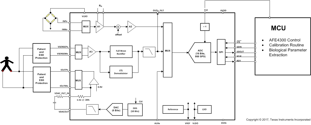
A typical application of the AFE4300 is a weight scale, as shown in Figure 14, that includes a weight measurement as well as a body impedance measurement with the architecture.
 Figure 14. Weight Scale Application
The weight applied on a load-cell generates the differential voltage that is converted by the weight scale signal chain of the AFE. For the body impedance measurement, a sinusoidal current (most commonly at a frequency of 50 kHz) is injected into a pair of electrodes that make contact with the human body. Two more electrodes serve as sense electrodes and the differential voltage developed across the sense electrodes is measured and digitized by the AFE. The whole system is clocked using an external clock source.
8.2.1 Design Requirements
Table 5 shows the typical requirements of a weight scale design using the AFE.
Table 5. Weight Scale Design Requirements
8.2.2 Detailed Design Procedure
A body impedance measurement is usually performed using four electrodes: a pair of excitation electrodes and a pair of sense electrodes. Body contact to each electrode involves a series impedance resulting from the skin-electrode interface. On the excitation side, this contact impedances come in series with the body impedance and cause the voltage swing on the excitation terminals of the AFE to increase. Excessive contact impedances on the excitation electrodes can therefore cause the excitation amplifier to saturate even while measuring normal ranges of body impedance. On the sense electrodes, the input impedance of the receiver is 50 kΩ. As a result, the contact impedances on the sense electrodes cause a small attenuation in the effective signal input to the receiver. For these reasons, the ac contact impedance at the excitation frequency must be minimized on both the excitation and sense electrodes.
To deduce an accurate impedance value from the AFE output in the body impedance measurement requires calibration relative to known impedances. Calibration is usually performed by measuring two or more known impedances and by constructing a piece-wise linear curve between the AFE output and the impedance.
To conserve power when not used, the AFE can be put in a sleep mode in which all signal chains are powered down. This mode reduces the average power consumption significantly. When the user issues a power-up interrupt (pressing a button or so forth) to the system, the AFE can be programmed to come out of sleep mode, perform the measurement, and go back to sleep again. To account for drifts with time, TI recommends that calibration be done every time the AFE is woken up. For the BCM measurement, TI recommends measuring the calibration impedances before every fresh measurement of body impedance. For the weight scale measurement, TI recommends measuring the channel offset (the AFE output without any load) before the measurement of the load. Also after every wake-up, provide sufficient time for the signal chain to settle before doing any measurements.
To meet product-level ESD requirements, additional external ESD protection diodes may need to be used to protect the AFE pins that interface with the electrodes.
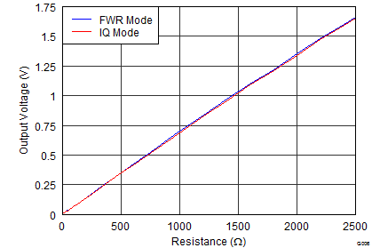
8.2.3 Application Curve
Figure 15 shows the linearity of the BCM up to 2.5 kΩ. As seen the figure, the maximum impedance that can be measured for the default configuration using the AFE4300 is typically 2.5 kΩ. However for better performance, TI suggests limiting the impedance to 1175 Ω. If higher impedance must be measured, the excitation current can be reduced by placing an external resistor of 1.5 kΩ (between DACOUT and DAC_FILT_IN), which increases the range by roughly 2x.
