TIDUEB8C July 2018 – March 2021 TPS274160
- Description
- Resources
- Features
- Applications
- 5
- 1System Description
- 2System Overview
- 3Hardware, Software, Testing Requirements, and Test Results
- 4Design Files
- 5Software Files
- 6Related Documentation
- 7About the Author
- 8Revision History
2.2.4 INA253
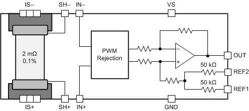
The INA253 features a 2-mΩ, precision, current-sensing resistor and a 80-V common-mode, zero-drift topology, precision, excellent common-mode rejection ratio (CMRR), and features enhanced pulse width modulation (PWM) rejection current-sensing amplifier integrated into a single package. High precision measurements are enabled through the matching of the shunt resistor value and the current-sensing amplifier gain providing a highly-accurate, system-calibrated solution. Enhanced PWM rejection reduces the effect of common-mode transients on the output signal that are associated with PWM signals. Multiple gain versions are available to allow for the optimization of the desired full-scale output voltage based on the target current range expected in the application.
 Figure 2-5 INA253 Block Diagram
The device has following key features:
- Precision integrated shunt resistor
- Shunt resistor: 2 mΩ
- Shunt resistor tolerance: 0.1% (maximum)
- ±15 A continuous from –40°C to 85°C
- 0°C to 125°C temperature coefficient: 10 ppm/°C
- Accuracy:
- Gain error: 0.25% (maximum)
- Gain drift: 10 ppm/°C (maximum)
- Offset voltage: ±2 mA
- Offset drift: 125 µA/°C (maximum)
- Wide common-mode range: –4 V to 80 V
- Available gains: 100 mV/A, 200 mV/A, and 400 mV/A