TIDT316 December 2022
- Description
- Features
- Applications
- 1Test Prerequisites
- 2Testing and Results
- 3Waveforms
- A Output Ripple Reduction, Output Current Capability, and Dithering Option
A.2 Maximum Output Current Capability at Ultra-Low Cold Cranking Using LM5157
With assembled ORing diodes (D2, D3) at bias input and disabled UVLO (R5 = OPEN), the circuit starts to switch at input voltage higher than 3 V.
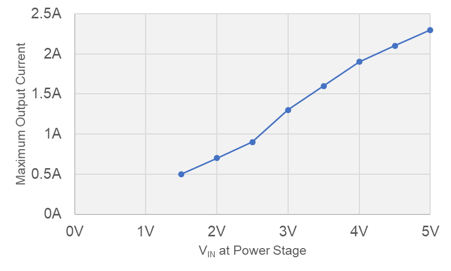
Table 4-1 shows the achievable output current at low-input voltages. Figure 4-4 represents the result from the table graphically for the input voltage at the power stage.
Table 4-1 Maximum Output Current at Low
Input Voltages
| Input Voltage at Power Stage | Board Input Voltage | Maximum Output Current |
|---|---|---|
| 1.5 V | 1.6 V | 500 mA |
| 2.0 V | 2.1 V | 700 mA |
| 2.5 V | 2.7 V | 900 mA |
| 3.0 V | 3.2 V | 1.3 A |
| 3.5 V | 3.7 V | 1.6 A |
| 4.0 V | 4.2 V | 1.9 A |
| 4.5 V | 4.6 V | 2.1 A |
| 5.0 V | 5.1 V | 2.3 A |
A peak load capability of 2 A is achieved at input voltages higher than 4.5 V.
 Figure 4-4 Maximum Output Current vs
Power Stage Input Voltage