TIDT307 October   2022


  1.   Description
  2.   Features
  3.   Applications
  4. 1Test Prerequisites
    1. 1.1 Voltage and Current Requirements
    2. 1.2 Considerations
    3. 1.3 Dimensions
  5. 2Testing and Results
    1. 2.1 Efficiency Graphs 9 VIN
    2. 2.2 Efficiency Data
    3. 2.3 Output Voltage Regulation (9 VIN)
    4. 2.4 Thermal Images
  6. 3Waveforms
    1. 3.1 Switching
      1. 3.1.1 Primary Side
      2. 3.1.2 Secondary Side
    2. 3.2 Output Voltage Ripple
    3. 3.3 Start-Up Sequence

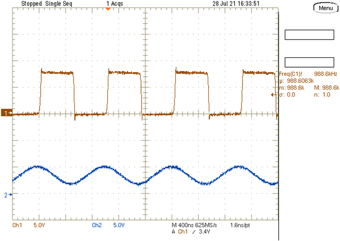
Secondary Side

GUID-20220926-SS0I-HGBF-JZRB-BZG3HH3RDRVD-low.png Figure 3-2 Switching Waveforms on Secondary Side
  • Ch1: A6 to –Vo2 at 9 VIN and 150-mA load current [scale: 5.0 V / div, 400 ns / div]
  • A3 to –Vo2 at 9 VIN and 150-mA load current [scale: 5.0 V / div, 400 ns / div]