TIDT272 April   2022


  1.   Description
  2.   Features
  3.   Applications
  4. 1Test Prerequisites
    1. 1.1 Voltage and Current Requirements
    2. 1.2 Considerations
    3. 1.3 Dimensions
  5. 2Testing and Results
    1. 2.1 Efficiency Graphs
    2. 2.2 Efficiency Data
    3. 2.3 Load Regulation
      1. 2.3.1 Primary Output
      2. 2.3.2 Secondary Outputs
        1. 2.3.2.1 Positive Outputs
        2. 2.3.2.2 Negative Outputs
    4. 2.4 Line Regulation
      1. 2.4.1 Primary Output
      2. 2.4.2 Secondary Outputs
        1. 2.4.2.1 Positive Outputs
        2. 2.4.2.2 Negative Outputs
    5. 2.5 Thermal Images
    6. 2.6 Bode Plots
      1. 2.6.1 5.5-V Input Voltage
      2. 2.6.2 12-V Input Voltage
  6. 3Waveforms
    1. 3.1 Switching
      1. 3.1.1 Q1 Drain to GND
      2. 3.1.2 Q1 Gate to GND
      3. 3.1.3 Diode D12
      4. 3.1.4 Diode D9
    2. 3.2 Output Voltage Ripple
      1. 3.2.1 Primary 10 V (Auxiliary)
      2. 3.2.2 Secondary +15 V
      3. 3.2.3 Secondary –5 V
    3. 3.3 Input Voltage Ripple
    4. 3.4 Start-Up Sequence
    5. 3.5 Shutdown Sequence

Shutdown Sequence

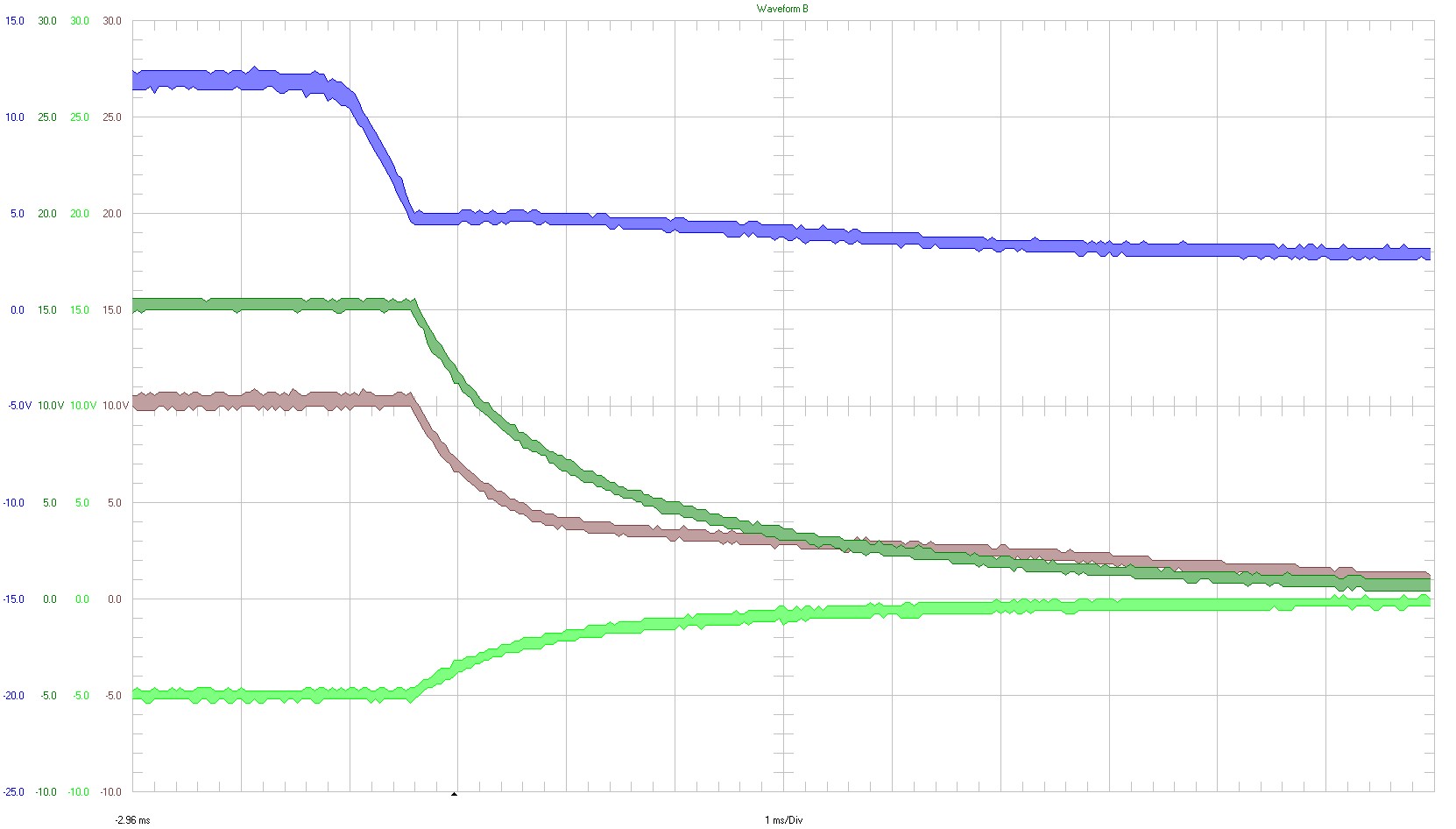
Shutdown behavior is shown in the following figure. An oscilloscope with isolated channels was used.

GUID-20220324-SS0I-WWGG-ZNDQ-VXJPHCXDJL9J-low.jpg

5 V / div

Ch1 ⇒ Input

Ch2 ⇒ +15 Vout (3)

Ch3 ⇒ +10 Vout (aux)

Ch4 ⇒ -5 Vout (3)

20 MHz bandwidth

1 ms / div

Figure 3-10 Shutdown