TIDT257A February   2022  – October 2022


  1.   Description
  2.   Features
  3.   Application
  4. 1Test Prerequisites
    1. 1.1 Voltage and Current Requirements
    2. 1.2 Considerations
    3. 1.3 Dimensions
  5. 2Testing and Results
    1. 2.1 Efficiency Graphs
    2. 2.2 Efficiency Data
      1. 2.2.1 THD Optimization
    3. 2.3 Thermal Images
      1. 2.3.1 Low-Side GaN Junction Temperature
    4. 2.4 Thermal Mechanical Design
      1. 2.4.1 Design Parameters
      2. 2.4.2 Thermal Resistance Calculation
      3. 2.4.3 Heat-Sink Diagrams
    5. 2.5 EMI
  6. 3Waveforms
    1. 3.1 AC Drop
    2. 3.2 Load Transients
    3. 3.3 Start-Up Sequence

Start-Up Sequence

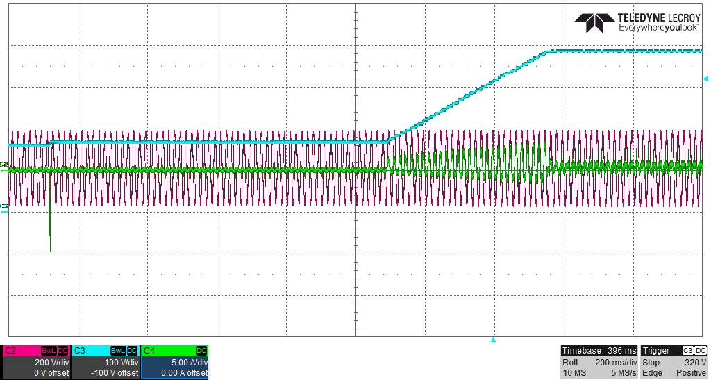
The waveforms in Figure 3-15 and Figure 3-16 were captured at 120 VAC, no load.

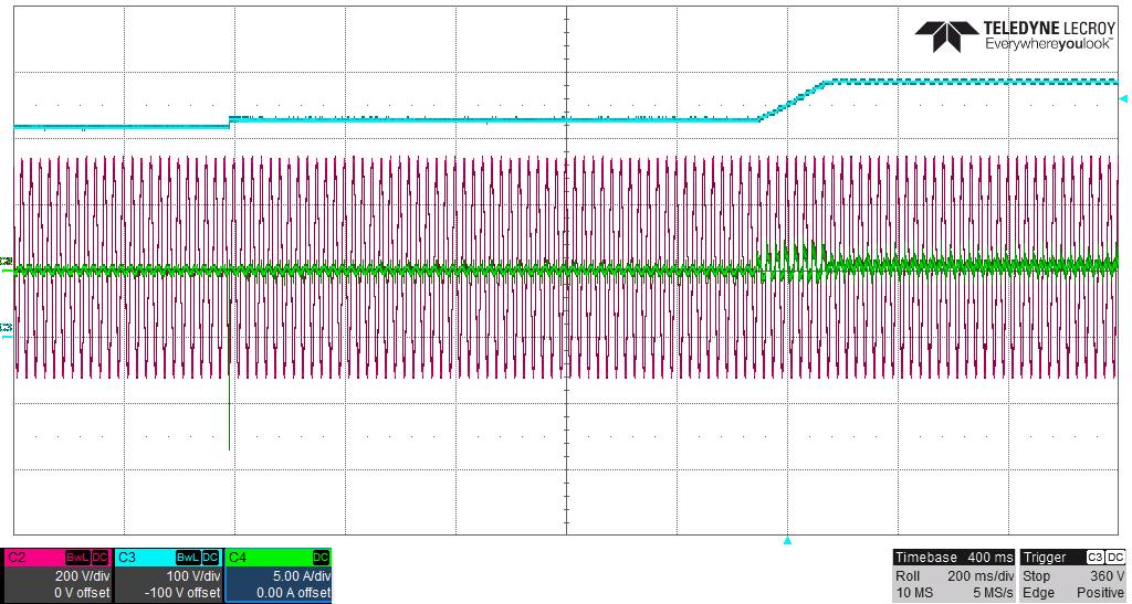
C2 = VAC, C3 = VOUT, C4 = IAC
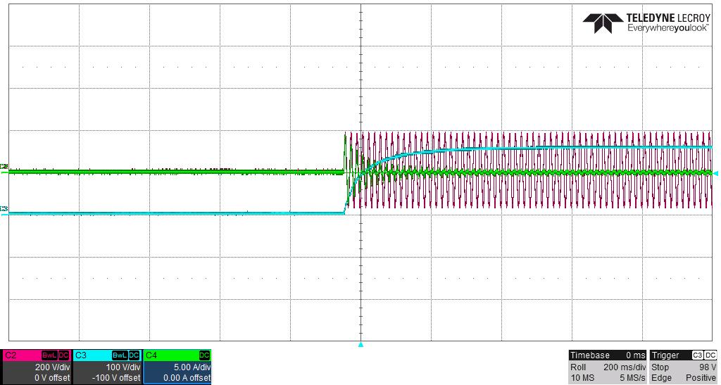
GUID-20220217-SS0I-ZLT1-GQ34-CLVL1LH5DZDT-low.jpgFigure 3-15 AC On
GUID-20220217-SS0I-XJ18-FL9C-DQP8BFHS6FPN-low.jpgFigure 3-16 Relay On

The waveforms in Figure 3-17 and Figure 3-18 were captured at 230 VAC, no load.
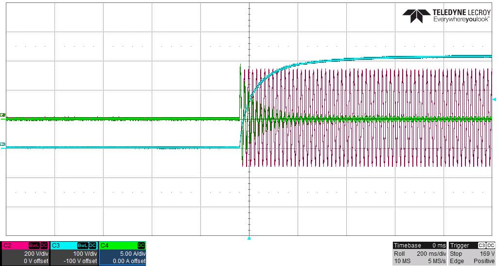
GUID-20220217-SS0I-7LHB-GMFF-ZGDJGW40FNFJ-low.jpgFigure 3-17 AC On
GUID-20220217-SS0I-VSTC-RSSV-PZDPN2D2L798-low.jpgFigure 3-18 Relay On