TIDT257A February 2022 – October 2022
2.3 Thermal Images
Conditions
- Same as efficiency test
- Input: 230 VAC
- Output: 380 V, 3.6 kW
- Frequency: 65 kHz
- Slew rate: 100 V/ns
- Dead-time: 100 ns
- Fan: FFB0412EN-00
- Air-speed: 33 LFM, 6 m/s
- Time: 30 minutes
Table 2-3 Heat Sink and Thermal
Interface
| GaN Heat Sink | GaN TIM | Silicon Heat Sink | Silicon TIM |
|---|---|---|---|
| S08EDR03-A | T-Work9000 | S08EDR08 | Tgard TNC-4(1) |
(1) Silicon TIM used in room
temperature test is LI2000A-150-150-0.2. Not recommended for worst case
conditions. Contact TI for heat-sink drawings.
Note: The thermal design
is based on 16-ARMS input current.
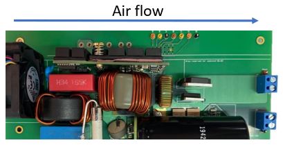 Figure 2-4 Test Setup
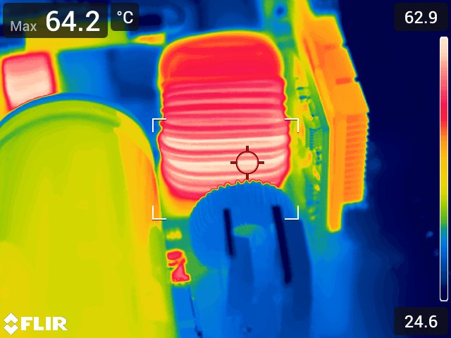 Figure 2-5 PFC Inductor
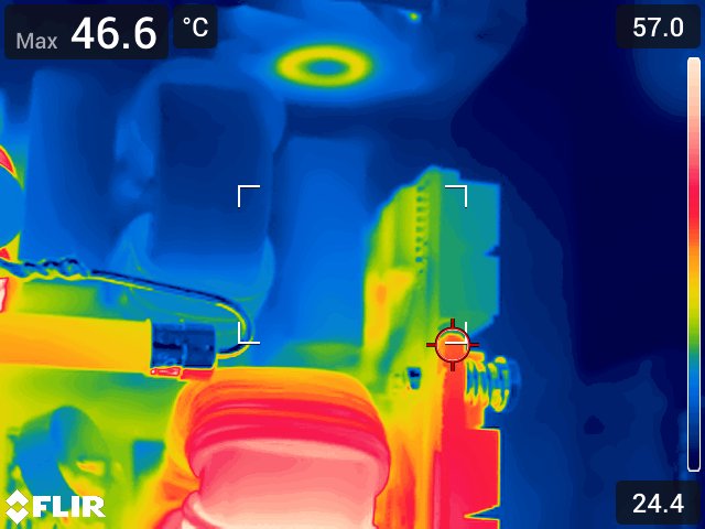 Figure 2-7 LF Silicon FETs
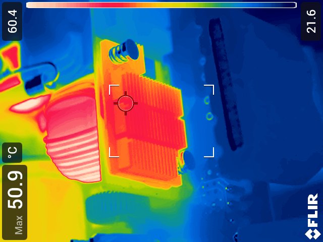 Figure 2-6 Backside of FET
Card
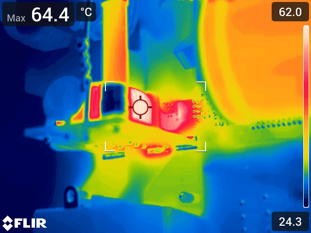 Figure 2-8 Common-Mode Choke and Hall
Sensor