• Menu
  • Product
  • Email
  • PDF
  • Order now
  • GaN-Based, 6.6-kW, Bidirectional, Onboard Charger Reference Design

    • TIDT249 September   2021


  • CONTENTS
  • SEARCH
  • GaN-Based, 6.6-kW, Bidirectional, Onboard Charger Reference Design
  1. 1Description
  2. 2Test Prerequisites
    1. 2.1 Voltage and Current Requirements
    2. 2.2 Required Equipment
    3. 2.3 Dimensions
  3. 3Test Results
    1. 3.1 Efficiency
    2. 3.2 System Performance
    3. 3.3 Bode Plots
    4. 3.4 Efficiency and Regulation Data
    5. 3.5 Thermal Data
  4. 4Waveforms
    1. 4.1 PFC Waveforms
    2. 4.2 CLLLC Waveforms
  5. IMPORTANT NOTICE
search No matches found.
  • Full reading width
    • Full reading width
    • Comfortable reading width
    • Expanded reading width
  • Card for each section
  • Card with all content


TEST REPORT

GaN-Based, 6.6-kW, Bidirectional, Onboard Charger Reference Design

1 Description

The PMP22650 reference design is a 6.6-kW, bidirectional, onboard charger. The design employs a two-phase totem pole PFC and a full-bridge CLLLC converter with synchronous rectification. The CLLLC utilizes both frequency and phase modulation to regulate the output across the required regulation range. The design uses a single processing core inside a TMS320F28388D microcontroller to control both the PFC and CLLLC. Synchronous rectification is implemented via the same microcontroller with Rogowski coil current sensors. High density is achieved through the use of high-speed GaN switches (LMG3522). The PFC is operating at 120 kHz and the CLLLC runs with a variable frequency from 200 kHz to 800 kHz. A peak system efficiency of 96.5% was achieved with an open-frame power density of 3.8 kW/L.

While the design calculations were done for a 6.6-kW output power, the design represents a suitable starting point for a 7.x-kW (for example, 7.2-kW to 7.4-kW) rated OBC operating from a 240-V input with a 32-A breaker.
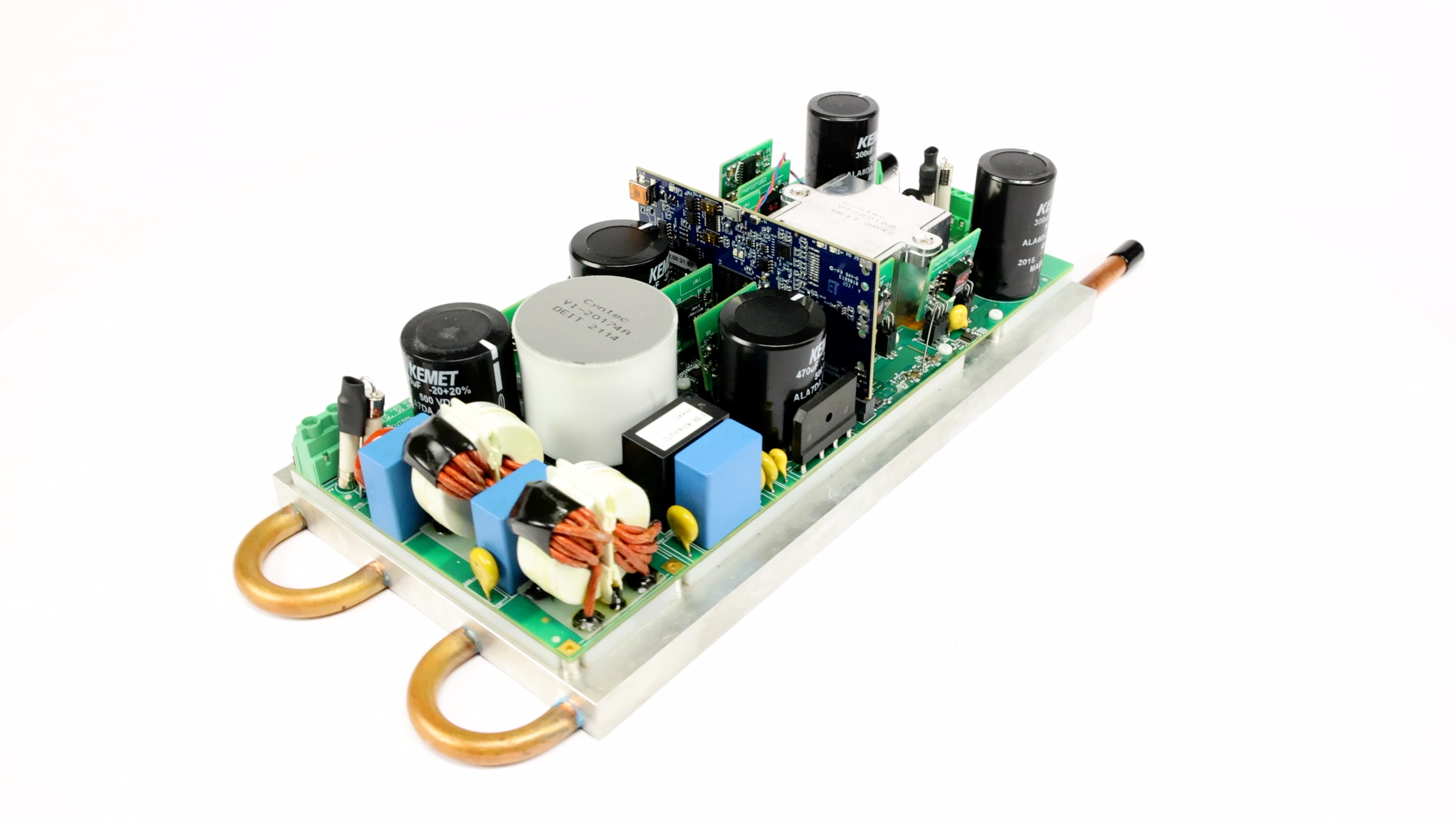
GUID-20210812-SS0I-PN8S-QVH9-TGNRGWQ9BZFH-low.jpgFigure 1-1 OBC Front View
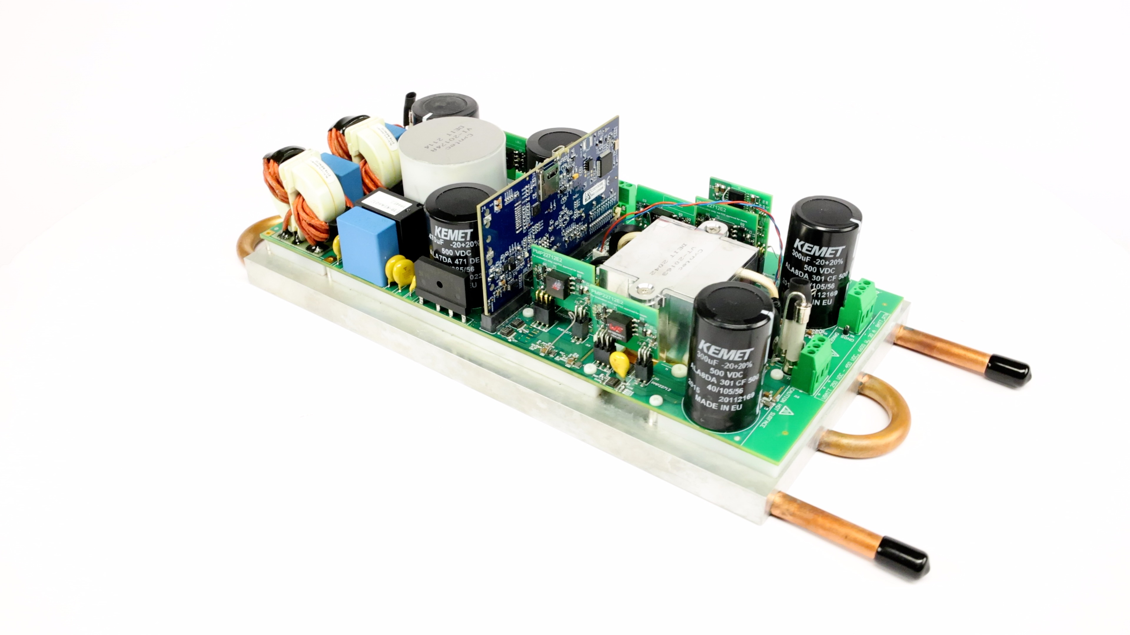
GUID-20210812-SS0I-QKF2-BN0S-DVZN2ZCSTSBN-low.jpgFigure 1-2 OBC Back View
GUID-20210812-SS0I-CFFS-QD3N-1GBC3N1PHZKZ-low.pngFigure 1-3 Simplified Schematic

2 Test Prerequisites

2.1 Voltage and Current Requirements

Table 2-1 Voltage and Current Requirements
Parameter Min Typ Max Units
AC Input Voltage 90 240 264 V
AC Input Current 32 A
DC Output Voltage 250 400 450 V
DC Output Current (Constant Current mode) 20 A
DC Output Power (Constant Power mode), VIN > 210 VRMS 6.6 kW

2.2 Required Equipment

  • 240 VAC, 7 kW AC source
  • 250 V to 450 V, 6.6 kW DC load
  • 12 V, 2 A bias supply
  • Refrigerated recirculating chiller

2.3 Dimensions

Total volume: 105.8 in3

  • Red region
    • All top-side components except output bulk capacitors
    • 113 mm × 241 mm × 50 mm
  • Blue region
    • Output bulk capacitors
    • 113 mm × 30 mm × 52 mm
  • Green region
    • PCB and bottom-side components
    • 113 mm x 271 mm x 6.4 mm
GUID-20210812-SS0I-M3NX-FJLK-HS9TBL0DZCDT-low.pngFigure 2-1 Solution Dimensions

3 Test Results

The power density achieved in this design is 3.8 kW/L (62.5 W/in3). The total system efficiency is 96.5%. The PFC has an efficiency of 98.5% and the CLLLC is 98%.

3.1 Efficiency

Efficiency data is provided in the following graphs with and without 12-V bias power. The bias supplies power to control, isolators, and gate drive. The graph in Figure 3-1 was taken under the following conditions:

  • VIN,RMS = 240 V
  • VOUT = 400 V
  • Coolant Temperature: 20°C
GUID-20210812-SS0I-TFBB-KCWD-TDRLL08DX1DN-low.pngFigure 3-1 PFC Efficiency

The graph in Figure 3-2 was taken under the following conditions:

  • VIN = 400 V
  • VOUT = 350 V
  • Coolant Temperature: 20°C
GUID-20210812-SS0I-QSSK-D7BD-ZBKSQPZ3LCXN-low.pngFigure 3-2 CLLLC Efficiency

The graph in Figure 3-3 was taken under the following conditions:

  • VIN,RMS = 240 V
  • VOUT = 350 V
  • Coolant Temperature: 20 °C
GUID-20210812-SS0I-LZPV-GHVH-N0HQ4CM28VVN-low.pngFigure 3-3 System Efficiency

3.2 System Performance

The following figures summarize the total system efficiency, system losses, total harmonic distortion (THD), and the normalized output voltage regulation accuracy.

The power density achieved in this design is 3.8 kW/L (62.5 W/in3). This comes with a total system efficiency of 96.5%. Loads above 1.5 kW have a THD < 5% and the regulation accuracy of the output voltage is roughly within ±0.06%.

The graphs in Figure 3-4 use the following conditions:

  • VIN,RMS = 240 V
  • VOUT = 350 V
  • Coolant Temperature: 20 °C
GUID-20210812-SS0I-M1DX-G231-VVN2BX2CQXH3-low.pngFigure 3-4 System Performance

3.3 Bode Plots

The following bode plots were acquired using the onboard software frequency response analyzer inside the TMS320F28388D microcontroller. The load used in the tests was configured as a constant current sink. The microcontroller is configured to regulate a constant output voltage. The bandwidth is roughly from 1 kHz to 2.5 kHz with a phase margin in excess of 45°.

GUID-20210812-SS0I-XWLS-5HLG-CM0MBCPWJBG9-low.png Figure 3-5 Voltage Loop Bode Plot

The following bode plots were acquired using the onboard software frequency response analyzer inside the TMS320F28388D microcontroller. The load used in the tests was configured as a constant voltage. The microcontroller is configured to regulate a constant output current. The bandwidth is roughly from 1 kHz to 2.5 kHz with a phase margin in excess of 60°.

GUID-20210812-SS0I-4PBP-9NFT-KTDWWBB4XBN0-low.png Figure 3-6 Voltage Loop Bode Plot (Constant Voltage Load)

3.4 Efficiency and Regulation Data

The following table shows efficiency and regulation data.

VOUT (V)

IOUT (A)

POUT (W)

VIN (V)

IIN (A)

PIN (W)

VBIAS (V)

IBIAS (A)

PBIAS (W)

Eff (%) No Bias

Eff (%) With Bias

352.76

0.5

177.35

240.12

1.17

215.36

11.92

1.24

14.73

82.35

77.08

352.74

1

354.12

240.05

1.79

391.84

11.92

1.23

14.67

90.37

87.11

352.72

1.5

530.65

239.98

2.49

572.25

11.92

1.24

14.8

92.73

90.39

352.71

2

706.27

239.91

3.23

753.97

11.92

1.24

14.78

93.67

91.87

352.7

2.5

882.52

239.84

3.97

936.83

11.92

1.24

14.76

94.2

92.74

352.7

3

1058.9

239.76

4.72

1118.95

11.92

1.23

14.71

94.63

93.41

352.7

3.5

1235.3

239.69

5.48

1301.58

11.92

1.23

14.65

94.91

93.85

352.69

4

1411.74

239.62

6.23

1484.44

11.92

1.23

14.61

95.1

94.18

352.69

4.5

1587.99

239.55

6.99

1667.43

11.92

1.22

14.57

95.24

94.41

352.69

5

1763.62

239.47

7.75

1849.94

11.92

1.22

14.51

95.33

94.59

352.69

5.5

1939.96

239.4

8.51

2031.56

11.93

1.21

14.48

95.49

94.82

352.69

6

2116.85

239.32

9.27

2212.59

11.93

1.21

14.48

95.67

95.05

352.68

6.5

2293.18

239.25

10.02

2392.72

11.93

1.21

14.46

95.84

95.26

352.68

7

2469.51

239.17

10.78

2572.43

11.93

1.21

14.4

96

95.46

352.67

7.5

2645.17

239.1

11.53

2751.5

11.93

1.19

14.16

96.14

95.64

352.68

8

2821.8

239.02

12.29

2931.48

11.94

1.16

13.85

96.26

95.81

352.69

8.5

2998.24

238.95

13.04

3111.5

11.94

1.14

13.56

96.36

95.94

352.71

9

3174.78

238.87

13.8

3292.5

11.95

1.11

13.26

96.43

96.04

352.72

9.5

3350.46

238.79

14.56

3472.6

11.95

1.09

12.99

96.48

96.12

352.76

10

3527.33

238.71

15.33

3654.7

11.95

1.07

12.76

96.51

96.18

352.79

10.5

3704.19

238.63

16.09

3837.2

11.96

1.05

12.52

96.53

96.22

352.84

11

3881.08

238.54

16.87

4020.3

11.96

1.03

12.37

96.54

96.24

352.91

11.5

4058.4

238.46

17.64

4204.2

11.96

1.02

12.24

96.53

96.25

352.92

12

4235

238.37

18.42

4387.9

11.96

1.02

12.16

96.51

96.25

352.93

12.5

4411.3

238.28

19.2

4571.5

11.96

1.01

12.08

96.5

96.24

352.96

13

4588.2

238.18

19.98

4756

11.96

1

12

96.47

96.23

352.99

13.5

4765.1

238.09

20.77

4940.9

11.96

1

11.92

96.44

96.21

353

14

4941.9

237.99

21.55

5125.8

11.97

0.99

11.86

96.41

96.19

353.02

14.5

5118.9

237.89

22.34

5311.4

11.97

0.99

11.79

96.38

96.16

353.02

15

5294.8

237.79

23.13

5496.4

11.97

0.98

11.73

96.33

96.13

353.02

15.5

5471.6

237.68

23.92

5682.4

11.97

0.98

11.69

96.29

96.09

353.03

16

5648.3

237.62

24.71

5868.9

11.97

0.97

11.64

96.24

96.05

353.05

16.5

5825.2

237.51

25.51

6056.1

11.97

0.97

11.59

96.19

96

353.02

17.5

6176.6

237.26

27.13

6432.3

11.97

0.96

11.52

96.03

95.85

353.02

18

6353.2

237.14

27.94

6621.6

11.97

0.96

11.49

95.95

95.78

353.03

18.5

6529.8

237.01

28.76

6812.2

11.97

0.96

11.47

95.85

95.69

353.05

19

6706.8

236.87

29.59

7004.3

11.97

0.96

11.44

95.75

95.6

3.5 Thermal Data

The following image is taken under full load operation. All of the significant heat generation components are connected to the cold plate on the bottom side of the board. The hottest components visible in this image come from the common-mode inductors in the EMI filter. These parts have no access to the cold plate and receive all their cooling via the ambient air.

GUID-20210812-SS0I-LGDX-24VH-DT2BDJVHLWPN-low.jpgFigure 3-7 Top Side Thermal Image

GaN FET temperatures are provide by means of the onboard temperature sensors inside the LMG3522 devices. Under full load conditions, all FET temperatures are less than 75°C.

Table 3-1 lists the GaN FET temperature measurements under the following conditions:

  • VIN,AC: 240 V
  • VDC,LINK: 400 V
  • Coolant temperature: 33°C
Table 3-1 GaN FET Temperature Measurements
GaN FETTemperature (°C)
PFC66.8
CLLLC Primary (350 V/19 A)58.1
CLLLC Secondary (350 V/19 A59.5
CLLLC Primary (300 V/19 A)61.0
CLLLC Secondary (300 V/19 A)74.0

Figure 3-8 shows the critical transformer temperatures under the following conditions:

  • Coolant Temperature: 33°C
  • Transformer temperature measurement locations
    • PRI 1 - Measured on the inside surface of the primary winding
    • PRI 2 - Measured on the outside surface of the primary winding
    • SEC 1 - Measured on the inside surface of the secondary winding
    • SEC 2 - Measured on the outside surface of the secondary winding
    • CORE 1 - Measured on the top of the core center leg
    • CORE 2 - Measured on the bottom of the core center leg
    • CORE 3 - Measured on the side of the core
    • CORE 4 - Measured on the top of the core
GUID-20210812-SS0I-PSFC-VW2J-0F1G7JNTNNJL-low.pngFigure 3-8 CLLLC Transformer Temperatures

4 Waveforms

4.1 PFC Waveforms

Figure 4-1 shows the PFC input voltage and input current waveform measured at the following parameters:

  • Traces
    • C2: VIN
    • C4: IIN
  • Conditions
    • VIN = 208 V
    • VOUT = 400 V
    • ROUT = 43 Ω
GUID-20210812-SS0I-HZKG-XKBH-RWMXTSLGRDKS-low.jpgFigure 4-1 PFC Input Voltage and Input Current

Figure 4-2 shows the PFC GaN drain voltage waveform measured at the following parameters:

  • Traces
    • C1: GaN Switch Node Drain Voltage
    • C2: VIN
    • C4: IIN
  • Conditions
    • VIN = 208 V
    • VOUT = 400 V
    • ROUT = 43 Ω
GUID-20210812-SS0I-BGMR-T5G3-0TRVTP71SCTL-low.jpgFigure 4-2 PFC GaN Drain Voltage

A zoom-in of the GaN switch drain-to-source voltage transition is shown to be approximately 20 ns in Figure 4-3. This rapid transition comes from the low COSS of the LMG3522.

The waveform in Figure 4-3 was measured using the following parameters:

  • Traces
    • C1: GaN Switch Node Drain Voltage
    • C2: VIN
    • C4: IIN
  • Conditions
    • VIN = 208 V
    • VOUT = 400 V
    • ROUT = 43 Ω
GUID-20210812-SS0I-TD3G-1VTV-B0FSRWL5TGLK-low.jpgFigure 4-3 PFC GaN Drain Voltage - Transition

4.2 CLLLC Waveforms

Figure 4-4 shows CLLLC operation at 19 A (6.6 kW) under the following parameters:

  • Traces
    • C1: GaN Primary Switch Node Drain Voltage
    • C2: GaN Secondary Switch Node Drain Voltage
    • C3: Transformer Primary Current
    • C4: Transformer Secondary Current
  • Conditions
    • VIN = 400 V
    • VOUT = 350 V
    • IOUT = 19 A
GUID-20210812-SS0I-QF4N-3VBB-QDD9TNPXS0V1-low.png Figure 4-4 CLLLC Operation 19 A (6.6 kW)

Figure 4-5 shows CLLLC operation at 10 A and the following parameters:

  • Traces
    • C1: GaN Switch Node Drain Voltage Leg 1
    • C2: GaN Switch Node Drain Voltage Leg 2
    • C3: Transformer Primary Current
    • C4: Transformer Secondary Current
  • Conditions
    • VIN = 400 V
    • VOUT = 350 V
    • IOUT = 10 A
GUID-20210812-SS0I-WW4N-TKBJ-XHMBHHZPQZZM-low.jpg Figure 4-5 CLLLC Operation 10 A

A zoom-in of the GaN switch drain-to-source voltage transition is shown to be approximately 40 ns in Figure 4-6. This rapid transition comes from the low COSS of the LMG3522.

The waveform in Figure 4-6 is measured using the following parameters:

  • Traces
    • C1: GaN Switch Node Drain Voltage Leg 1
    • C2: GaN Switch Node Drain Voltage Leg 2
    • C3: Transformer Primary Current
    • C4: Transformer Secondary Current
  • Conditions
    • VIN = 400 V
    • VOUT = 350 V
    • IOUT = 10 A
GUID-20210812-SS0I-GMXM-3TZB-DK68W1V6Q3GS-low.jpg Figure 4-6 CLLLC Operation 10 A - GaN FET Transitions

The waveform in Figure 4-7 is measured using the following parameters:

  • Traces
    • C1: GaN Switch Node Drain Voltage Leg 1
    • C2: GaN Switch Node Drain Voltage Leg 2
    • C3: Transformer Primary Current
    • C4: Transformer Secondary Current
  • Conditions
    • VIN = 400 V
    • VOUT = 350 V
    • IOUT = 2 A
GUID-20210812-SS0I-ZW8N-BQWJ-7KHDN4J6MKL3-low.jpg Figure 4-7 CLLLC Operation 2 A

A zoom-in of the GaN switch drain-to-source voltage transition is shown to be approximately 75 ns in Figure 4-8. This rapid transition comes from the low COSS of the LMG3522. The slightly longer transition time in this image comes from the lighter load condition and the resulting reduced current flow.

The waveform in Figure 4-8 is measured using the following parameters:

  • Traces
    • C1: GaN Switch Node Drain Voltage Leg 1
    • C2: GaN Switch Node Drain Voltage Leg 2
    • C3: Transformer Primary Current
    • C4: Transformer Secondary Current
  • Conditions
    • VIN = 400 V
    • VOUT = 350 V
    • IOUT = 2 A
GUID-20210812-SS0I-T4PT-RKHC-XVDFTD0NQ7QJ-low.jpg Figure 4-8 CLLLC Operation 2 A - GaN FET Transitions

IMPORTANT NOTICE AND DISCLAIMER

TI PROVIDES TECHNICAL AND RELIABILITY DATA (INCLUDING DATASHEETS), DESIGN RESOURCES (INCLUDING REFERENCE DESIGNS), APPLICATION OR OTHER DESIGN ADVICE, WEB TOOLS, SAFETY INFORMATION, AND OTHER RESOURCES “AS IS” AND WITH ALL FAULTS, AND DISCLAIMS ALL WARRANTIES, EXPRESS AND IMPLIED, INCLUDING WITHOUT LIMITATION ANY IMPLIED WARRANTIES OF MERCHANTABILITY, FITNESS FOR A PARTICULAR PURPOSE OR NON-INFRINGEMENT OF THIRD PARTY INTELLECTUAL PROPERTY RIGHTS.
These resources are intended for skilled developers designing with TI products. You are solely responsible for (1) selecting the appropriate TI products for your application, (2) designing, validating and testing your application, and (3) ensuring your application meets applicable standards, and any other safety, security, or other requirements. These resources are subject to change without notice. TI grants you permission to use these resources only for development of an application that uses the TI products described in the resource. Other reproduction and display of these resources is prohibited. No license is granted to any other TI intellectual property right or to any third party intellectual property right. TI disclaims responsibility for, and you will fully indemnify TI and its representatives against, any claims, damages, costs, losses, and liabilities arising out of your use of these resources.
TI’s products are provided subject to TI’s Terms of Sale (www.ti.com/legal/termsofsale.html) or other applicable terms available either on ti.com or provided in conjunction with such TI products. TI’s provision of these resources does not expand or otherwise alter TI’s applicable warranties or warranty disclaimers for TI products.
Mailing Address: Texas Instruments, Post Office Box 655303, Dallas, Texas 75265
Copyright © 2021, Texas Instruments Incorporated


Texas Instruments

© Copyright 1995-2025 Texas Instruments Incorporated. All rights reserved.
Submit documentation feedback | IMPORTANT NOTICE | Trademarks | Privacy policy | Cookie policy | Terms of use | Terms of sale