SSZT472 june 2019 LMK04828 , LMK04832 , LMK61E2 , LMX2594
Next-generation aerospace and defense and test and measurement system bandwidths are moving from 10s to 100s of megahertz to multigigahertz of instantaneous bandwidths. Trends in phased-array radar, 5G wireless test systems, electronic warfare and digital oscilloscopes are pushing bandwidths higher and dramatically increasing the number of channels in a system.
These trends complicate signal-chain design, including the data converter, clocking and power supply. Selecting the appropriate data converter, synchronizing multiple channels, and optimizing your power supply are critical to achieving the necessary bandwidth across multiple channels.
Selecting Your Data Converter
- Will you use a zero intermediate frequency (IF)/complex mixer architecture (Figure 1)?
- Pros: the analog-to-digital converter (ADC) input bandwidth and sampling rates are lower than other architectures, and you can simplify or eliminate filtering.
- Cons: you need two ADC channels per antenna element for the I and Q paths and the mixer image may result in lower system performance.
- Will you use a heterodyne approach (Figure 2)?
- Pros: you need only a single data-converter channel and the ADC input bandwidth is lower than radio frequency (RF) sampling.
- Cons: it requires one or more mixers, the signal image and generated harmonics will complicate filtering, and it’s difficult to adjust the frequency of interest; you must move the Local Oscillator (LO).
- Will you use direct RF sampling (Figure 3)?
- Pros: you don’t need a mixer given the simplified signal chain, and it’s easy to adapt the frequency digitally using digital down converters (DDCs) and numerically controlled oscillators (NCOs).
- Cons: the highest signal frequency needs to be within the ADC’s input bandwidth, and you’ll need to do frequency planning to achieve the highest performance.
 Figure 1 Typical Complex Mixer
Architecture
 Figure 2 Typical Heterodyne
Architecture
 Figure 3 Typical RF sampling
architecture
Figure 3 Typical RF sampling
architecture- What is the widest bandwidth signal that you need to measure?
- At a minimum, the data converter will need a sampling rate of at least 2.5 times the instantaneous bandwidth of the signal for direct sampling, or 1.25 times for zero IF.
- For the best performance, a sampling rate of ~10 times the instantaneous bandwidth will allow you to more easily avoid signal harmonics and spurs.
TI’s RF-sampling frequency planner, analog filter and DDC Excel calculator can help with frequency planning and filtering requirements and show you the effects of complex digital decimation of your signal.
As I mentioned earlier, wideband systems need high-sampling-rate converters. For example, an RF sampling system with a signal bandwidth of 1 GHz would benefit from a data converter with a ~10-GSPS conversion speed to avoid signal harmonics. Until recently, TI’s fastest converter was the ADC12DJ3200, which is a 12-bit ADC that runs at 3.2 GSPS per channel in dual-channel mode or 6.4 GSPS in single-channel mode. But even in single-channel mode, it does not meet the desired 10-GSPS speed. So to meet this requirement, the Flexible 3.2 GSPS Multichannel AFE Reference Design for DSOs, RADAR and 5G Wireless Test Systems, shown in Figure 4, combines two ADC12DJ3200s on one board.
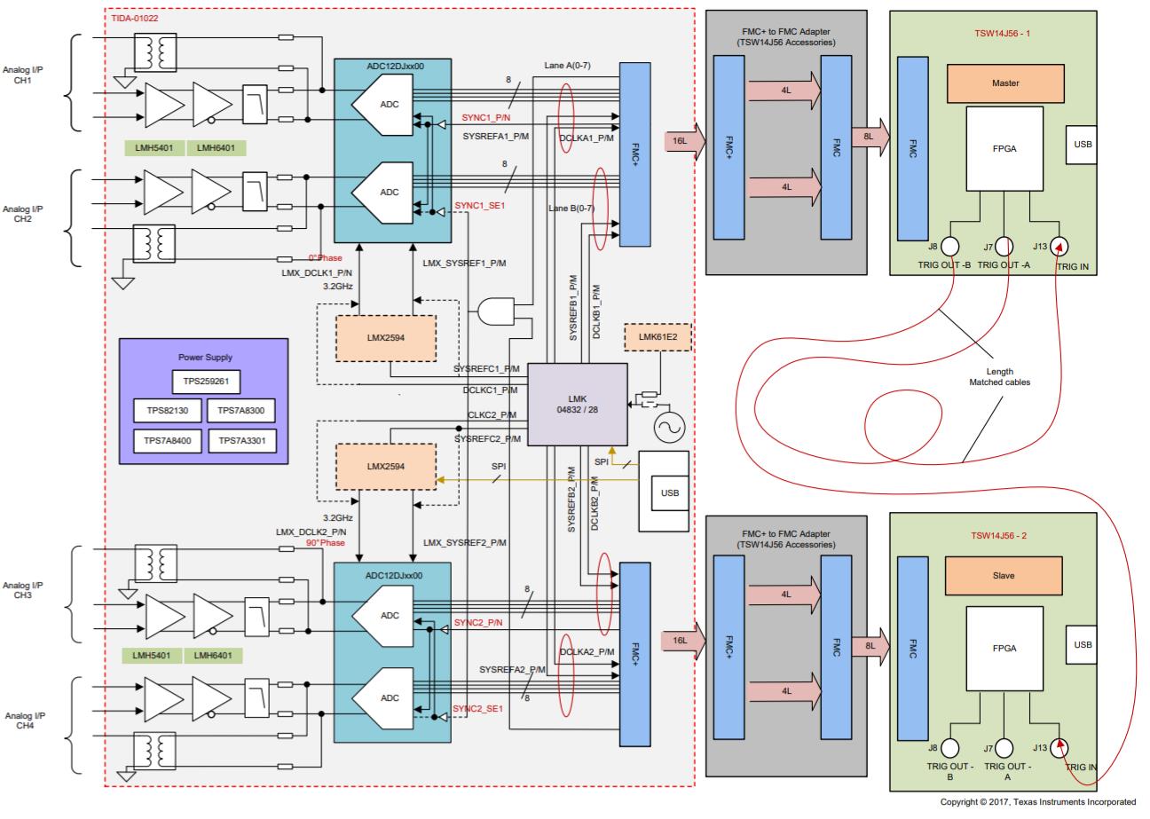 Figure 4 Multichannel AFE reference
design block diagram
Figure 4 Multichannel AFE reference
design block diagramThis reference design offers system flexibility, since it can run in quad-channel, 3.2-GSPS mode, dual-channel, 6.4-GSPS mode or as a single channel running at up to 12.8 GSPS. Our 12.8-GSPS analog front end reference design for high-speed oscilloscope and wide-band digitizer illustrates onboard interleaving of the two ADCs.
Now, with the introduction of our new dual-channel, 5.2-GSPS ADC12DJ5200RF, you have even more performance and flexibility for your next generation designs. Since the ADC12DJ5200RF is pin compatible with the ADC12DJ3200, we were quickly able to modify our existing reference design and can now offer a Scalable 20.8 GSPS reference design for 12-bit digitizers. At 20.8 GSPS, the entire 8-GHz input bandwidth of the device can be digitized in a single capture.
Clocking Your Design
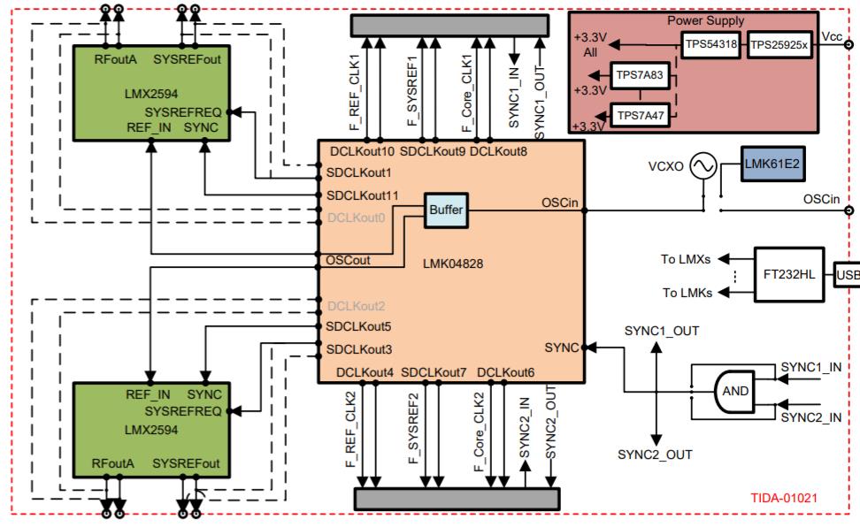 Figure 5 Multichannel JESD204B 15-GHz
Clocking Block Diagram
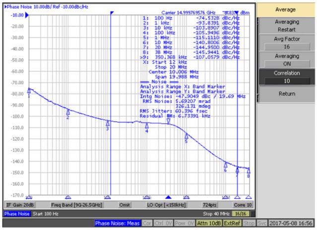 Figure 6 LMX2594 phase noise at 15
GHz
Figure 6 LMX2594 phase noise at 15
GHzAs configured, the board supports up to two data converters and two field-programmable gate arrays (FPGAs) but can easily be adapted to clock up to six converters and one FPGA. However, many systems require significantly more channels. For these situations, our High Channel Count JESD204B Clock Generation Reference Design for RADAR and 5G Wireless Testers and High Channel Count JESD204B Daisy Chain Clock Reference Design for RADAR and 5G Wireless Testers enable the operation of our clocks in either a tree structure, shown in Figure 7, or a daisy-chain configuration. Using these techniques, you can expand to thousands of channels with minimal degradation in system performance.
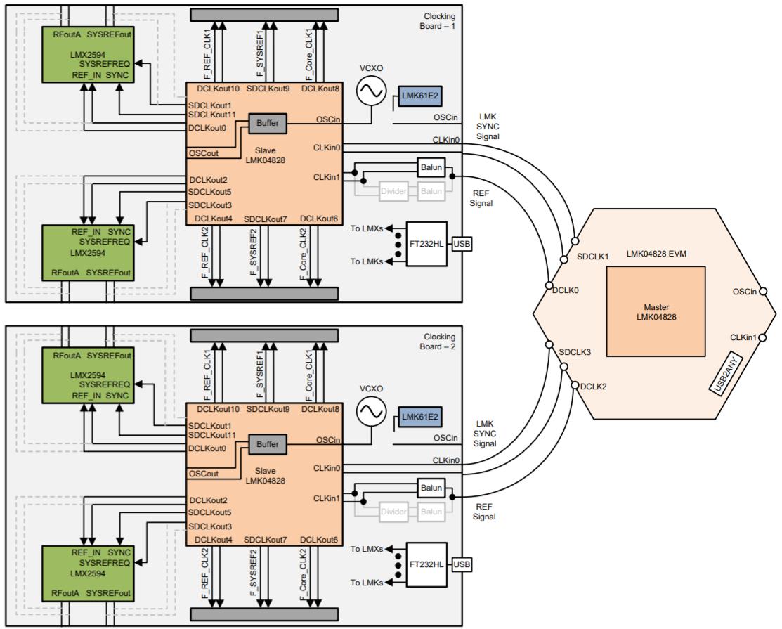 Figure 7 JESD204B Clock Generation
Reference Design Tree Structure Block Diagram
Figure 7 JESD204B Clock Generation
Reference Design Tree Structure Block DiagramPowering Your Design
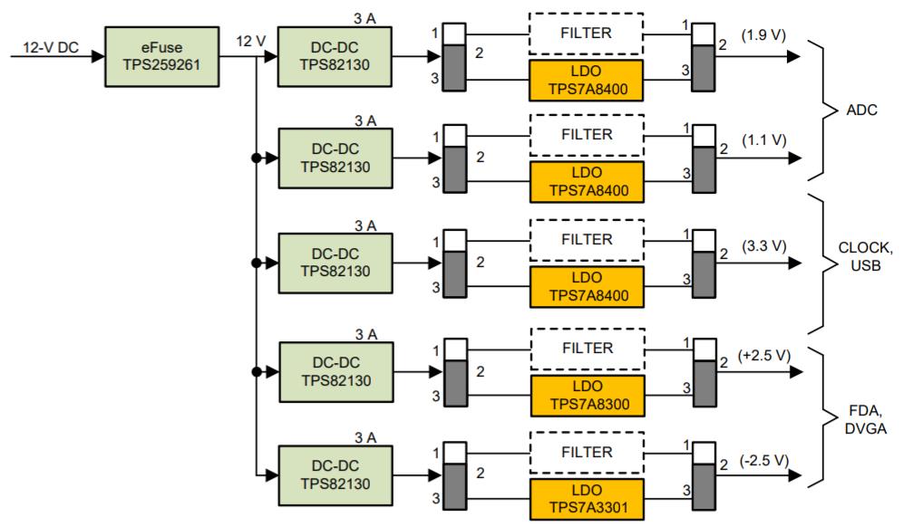 Figure 8 3.2-GSPS Multichannel AFE
Reference Design Power-supply Block Diagram
Figure 8 3.2-GSPS Multichannel AFE
Reference Design Power-supply Block DiagramThe board also includes a series of header pins along the top that enable you to bypass the onboard power solution with a new design, such as our Low noise power-supply reference design maximizing performance in 12.8 GSPS data acquisition systems. This reference design, shown in Figure 9, enables the synchronization of all DC/DC regulators to a master clock, making it easier to filter out converter switching noise. In addition, you can shift the phase of the clock to each converter so that all converters are not switching at the same time, lowering the total switching energy. Finally, the DC/DC converters on the reference design are more efficient, lowering the total power loss on the board. As with the original design, the LDOs can still be bypassed.
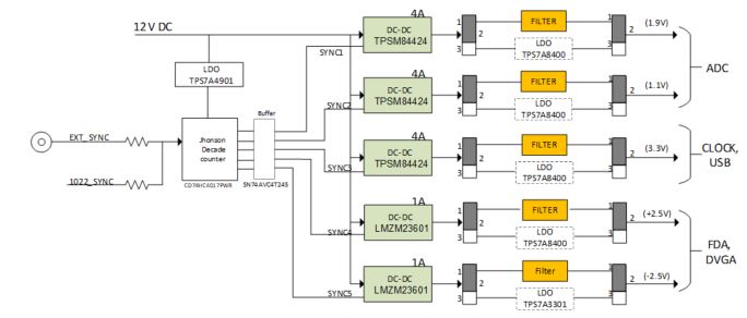 Figure 9 Low Noise Power Supply
Reference Design Block Diagram
Figure 9 Low Noise Power Supply
Reference Design Block DiagramYou can see that selecting the correct data converter is just one of your challenges. Once you’ve made that selection, it’s critical to select the best clock and power-supply designs in order to not degrade the performance of your costly data converter.
Additional Resources
- Check out our training video: Optimize Your RF Sampling ADC Receiver Performance with the Frequency and Sample Rate Planning Calculator.
- Check out TI’s full high-speed ADC and digital-to-analog converter portfolios.