SPRUIW4 October 2021 TMS320F280021 , TMS320F280021-Q1 , TMS320F280023 , TMS320F280023-Q1 , TMS320F280023C , TMS320F280025 , TMS320F280025-Q1 , TMS320F280025C , TMS320F280025C-Q1 , TMS320F280033 , TMS320F280034 , TMS320F280034-Q1 , TMS320F280036-Q1 , TMS320F280036C-Q1 , TMS320F280037 , TMS320F280037-Q1 , TMS320F280037C , TMS320F280037C-Q1 , TMS320F280038-Q1 , TMS320F280038C-Q1 , TMS320F280039 , TMS320F280039-Q1 , TMS320F280039C , TMS320F280039C-Q1
- Trademarks
- 1Feature Differences Between F28002x and F28003x
- 2PCB Hardware Changes
- 3Feature Differences for System Consideration
- 4Application Code Migration From F28002x to F28003x
- 5Specific Use Cases Related to F28003x New Features
- 6EABI Support
- 7References
1.1 F28002x and F28003x Feature Comparison
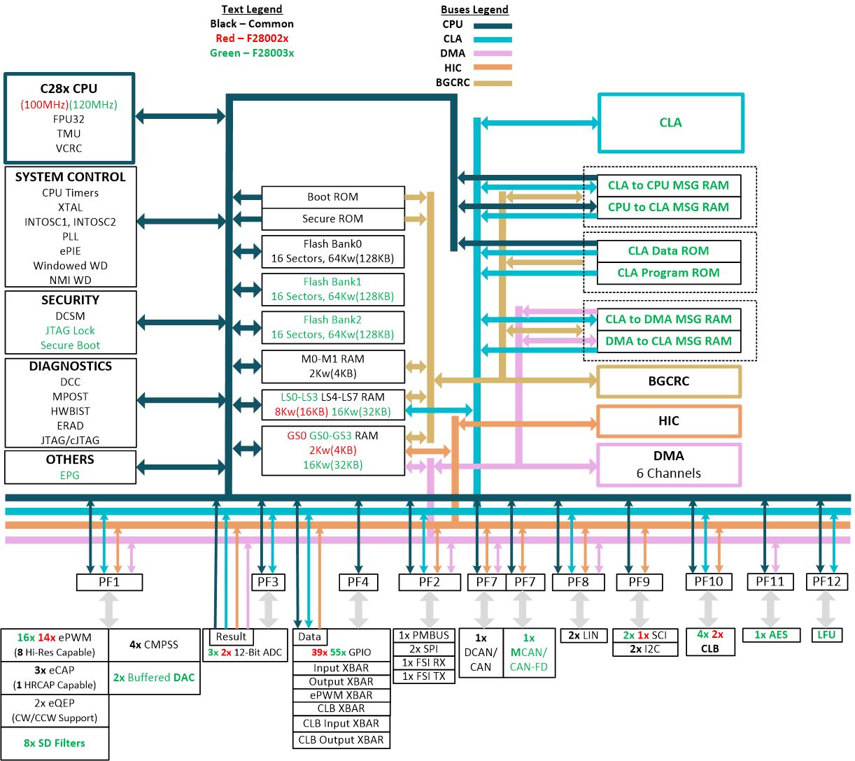
An overlaid block diagram of F28002x and F28003x is shown in Figure 1-1 while feature comparison of the superset part numbers for the F28003x and F28002x devices is shown in Table 1-1.
 Figure 1-1 F28003x and F28002x Overlaid
Functional Block Diagram
Figure 1-1 F28003x and F28002x Overlaid
Functional Block DiagramTable 1-1 F28002x and F28003x Superset
Device Comparison
| Feature | F28002x | F28003x | ||||||
|---|---|---|---|---|---|---|---|---|
| 80-Pin PN | 64-Pin PM | 48-Pin PT | 100-Pin PZ | 80-Pin PN | 64-Pin PM | 48-Pin PT | ||
| Processor and Accelerators | ||||||||
| C28x | Frequency (MHz) | 100 | 120 | |||||
| FPU | Yes (instructions for Fast Integer Division) | |||||||
| VCRC | Yes | |||||||
| TMU | Yes – Type 1 (instructions supporting NLPID) | |||||||
| CLA – Type 2 | Available | No | Yes | |||||
| Frequency (MHz) | - | 120 | ||||||
| 6–Channel DMA – Type 0 | Yes | |||||||
| External interrupts | 5 | |||||||
| Memory | ||||||||
| Flash | 128KB (64Kw) | 384KB (192Kw) | ||||||
| RAM | Dedicated | 4KB (2Kw) | ||||||
| Local Shared | 16KB (8Kw) | 32KB (16Kw) | ||||||
| Message | - | 1KB (0.5Kw) | ||||||
| Global Shared | 4KB (2Kw) | 32KB (16Kw) | ||||||
| Total | 24KB (12Kw) | 69KB (34.5Kw) | ||||||
| Message RAM Types | - | 512B (256w) CPU–CLA 512B (256w) CLA–DMA | ||||||
| ECC | FLASH, Mx, LSx | FLASH, Mx, LSx, GSx, Message RAM | ||||||
| Parity | GSx, ROM | ROM, CAN RAM | ||||||
| Code security for on–chip flash and RAM | Yes | |||||||
| System | ||||||||
| Configurable Logic Block (CLB) | 2 Tiles | 4 Tiles | ||||||
| Embedded Pattern Generator (EPG) | - | Yes | ||||||
| Motor Control Libraries in ROM | Yes | |||||||
| 32–bit CPU timers | 3 | |||||||
| Advance Encryption Standard (AES) | – | Yes | ||||||
| Background CRC (BGCRC) | Yes | |||||||
| Live Firmware Update (LFU) Support | – | Yes, with enhancements and flash bank erase time improvements | ||||||
| Secure Boot | – | Yes | ||||||
| JTAG Lock | – | Yes | ||||||
| HWBIST | Yes | |||||||
| Nonmaskable Interrupt Watchdog (NMIWD) timers | 1 | |||||||
| Watchdog timers | 1 | |||||||
| Crystal oscillator/External clock input | 1 | |||||||
| Internal oscillator | 2 | |||||||
| Pins and Power Supply | ||||||||
| Internal 3.3v to 1.2v Voltage Regulator | VREG LDO | Yes | ||||||
| GPIO pins | 39 | 26 | 14 | 51 | 39 | 26 | 14 | |
| Additional GPIO | 4 (2 from cJTAG and 2 from X1/X2) | |||||||
| AIO (analog with digital inputs) | 16 | 16 | 14 | 23 | 16 | 16 | 14 | |
| AGPIO (analog with digital inputs and outputs) | - | 2 | 2 | - | - | |||
| Analog Peripherals | ||||||||
| ADC 12–bit | Number of ADCs | 2 | 3 | |||||
| MSPS | 3.45 | 4 | ||||||
| Conversion Time (ns) | 290 | 250 | ||||||
| ADC channels (single–ended) - includes the two gpdac outputs on F28003x | 16 | 16 | 14 | 23 | 18 | 16 | 14 | |
| Temperature sensor | 1 | |||||||
| Buffered DAC | - | 2 | ||||||
| CMPSS (each CMPSS has two comparators and two internal DACs) | 4 | |||||||
| Control Peripherals | ||||||||
| eCAP/HRCAP modules | 3 (1 with HRCAP capability) – Type 2 | |||||||
| ePWM/HRPWM channels – Type 4 | 14 (8 with HRPWM) | 16 (8 with HRPWM) | ||||||
| eQEP modules | 2 – Type 2 | |||||||
| SDFM channels | - | 8 – Type 2 | ||||||
| Communication Peripherals | ||||||||
| CAN (DCAN) – Type 0 | 1 | |||||||
| CANFD (MCAN) – Type 1 | – | 1 | ||||||
| FSI | 1 (1 RX and 1 TX) – Type 1 | 1 (1 RX and 1 TX) – Type 2 | ||||||
| I2C – Type 1 | 2 | |||||||
| LIN – Type 1 | 2 | |||||||
| HIC | Yes - Type 0 | Yes - Type 1 | ||||||
| PMBus – Type 0 | 1 | |||||||
| SCI – Type 0 | 1 | 2 | ||||||
| SPI – Type 2 | 2 | |||||||
| Package Options, Temperature, and Qualification | ||||||||
| Junction temperature (TJ) | –40°C to 125°C | –40°C to 150°C | ||||||
| Free-Air temperature (TA) | –40°C to 125°C | |||||||
| Package Options with AEC-Q100 Qualification available | Yes | Yes | Yes | Yes | – | Yes | Yes | |