SPRAD13 May 2022 AM623 , AM625
- Abstract
- Trademarks
- 1 Introduction
- 2 Via Channel Arrays
- 3 Width/Spacing Proposal for Escapes
- 4 Stackup
- 5 Via Sharing
- 6 Floorplan Component Placement
- 7 Critical Interfaces Impact Placement
- 8 Routing Priority
- 9 SerDes Interfaces
- 10DDR Interfaces
- 11Power Decoupling
- 12Route Lowest Priority Interfaces Last
- 13Summary
13 Summary
The via channels have been carefully co-designed to ensure escapes for all signals and power while meeting the respective signal and power integrity goals for each interface. A summary of all via channel arrays and vias for the different signal and power supply nets is shown in Table 13-1.
Table 13-1 Via Channel Summary
| Net | #VCA | #Vias | #Pins |
|---|---|---|---|
| Signals | 146 | 146 | 146 |
| VSS | 21 | 20 | 43 |
| VDD_CORE | 11 | 11 | 17 |
| VDDR_CORE | 5 | 5 | 8 |
| VDDS_DDR | 4 | 4 | 4 |
| VDDSHV0 | 1 | 1 | 2 |
| VDDSHV1 | 1 | 1 | 2 |
| VDDSHV2 | 2 | 2 | 2 |
| VDDSHV3 | 2 | 2 | 4 |
| VDDSHV4 | 1 | 1 | 1 |
| VDDSHV5 | 1 | 1 | 1 |
| VDDSHV6 | 1 | 1 | 1 |
| VDDSHV_MCU | 1 | 1 | 2 |
| VDDSHV_CANUART | 1 | 1 | 1 |
| VDD_CANUART | 1 | 1 | 1 |
Notes:
- Outer two rows are fully fanned-out on top layer with no VCAs or Vias. This includes a handful of VSS balls (in the outer two rows) which are not included in the table.
- There are a total of 200 VCAs; one is not used (J15 location), one is used for routing (M14 for VSS), all others have a Via.
- Any net not specifically listed above is either fanned out directly on outer layer, or is counted in the “signals” row with 1 via per 1 pin (this includes VDDA_x and CAP_VDDx nets that are considered as power nets).
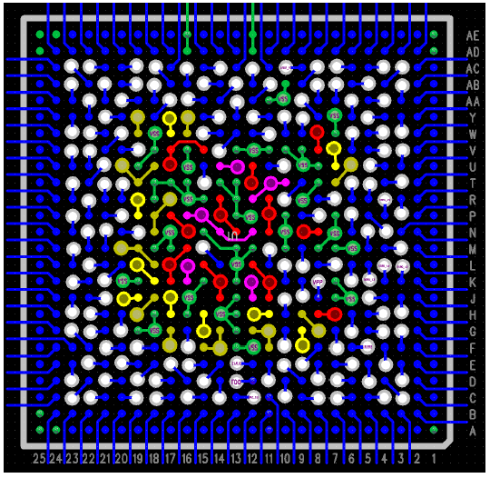
A picture showing AM62x with all signals and power escaped is shown in Figure 13-1.
An example layout file for the fully escaped design can be downloaded here.
 Figure 13-1 AM62x with Complete Signal and Power Escapes