SPRACY7 October 2021 TMS320F2800132 , TMS320F2800133 , TMS320F2800135 , TMS320F2800137 , TMS320F2800152-Q1 , TMS320F2800153-Q1 , TMS320F2800154-Q1 , TMS320F2800155 , TMS320F2800155-Q1 , TMS320F2800156-Q1 , TMS320F2800157 , TMS320F2800157-Q1 , TMS320F280033 , TMS320F280034 , TMS320F280034-Q1 , TMS320F280036-Q1 , TMS320F280036C-Q1 , TMS320F280037 , TMS320F280037-Q1 , TMS320F280037C , TMS320F280037C-Q1 , TMS320F280038-Q1 , TMS320F280038C-Q1 , TMS320F280039 , TMS320F280039-Q1 , TMS320F280039C , TMS320F280039C-Q1
3.2.6 Shift Right Once - CPOL=0, CPHA=0
In this example, once again the SHIFT right once mode is used, and the SIGGEN0_DATA0 and SIGGEN0_DATA1 registers are NOT loaded into the active SIGGEN data. Therefore, when SHIFT RIGHT ONCE mode is used, after BIT-LENGTH shifts are done, the IDLE signal level of the data line will be the first bit in the clock stream. The IDLE signal level of the clock line will be the DATA[32] bit which corresponds to SIGGEN0_DATA1[0].
//
// Data
//
#define SIG_GEN_DATA0_0_15    0b1111000011001111U

//
// Clock - Data latched on falling edge
//
#define SIG_GEN_DATA0_16_31   0b0101010101010101U

//
// During idle CLK is LOW
//
#define SIG_GEN_DATA1_0       0b0
When the device PinMux is configured to be driven by Output X-Bar (which is sourced from EPGOUT), while the SIGGEN module is not enable, the signal output on the GPIO is LOW (0). When the SIGGEN module is enabled for the very first time, the generated SPI clock signal will be low until the first "1" in the clock bit stream.
In all following transfers, the IDLE state of the clock before and after each pattern generation will always be LOW.
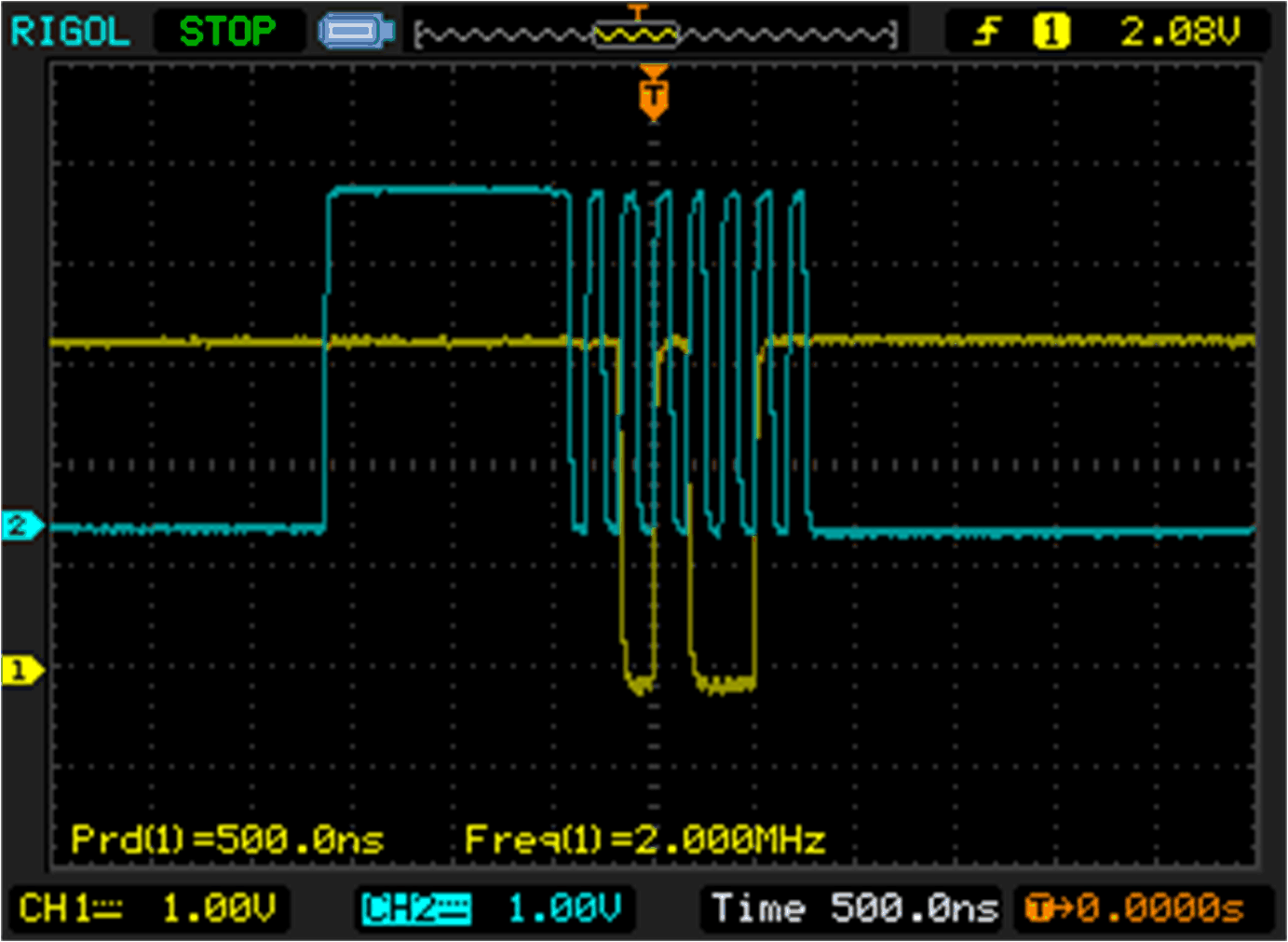
 Figure 3-18 Shift Right Once All Other
Data and Clock Generation - CPOL=0, CPHA=0
Figure 3-18 Shift Right Once All Other
Data and Clock Generation - CPOL=0, CPHA=0A zoomed in view of the data and clock generated relevant to each other is shown in Figure 3-19.
As it can be seen in all of the examples above, using the SHIFT/ROTATE right modes requires the bit streams placed in SIGGEN registers to be changed. The IDLE state for the data and clock patterns depend on which mode is selected. If the SHIFT mode is selected, the data IDLE state depends on the first bit of the clock bit stream. The user can configure the SIGGEN module to have a BIT-LENGTH of 17 to decouple the data signal's IDLE state bit from the clock bit stream's first bit.