SPRACY7 October 2021 TMS320F2800132 , TMS320F2800133 , TMS320F2800135 , TMS320F2800137 , TMS320F2800152-Q1 , TMS320F2800153-Q1 , TMS320F2800154-Q1 , TMS320F2800155 , TMS320F2800155-Q1 , TMS320F2800156-Q1 , TMS320F2800157 , TMS320F2800157-Q1 , TMS320F280033 , TMS320F280034 , TMS320F280034-Q1 , TMS320F280036-Q1 , TMS320F280036C-Q1 , TMS320F280037 , TMS320F280037-Q1 , TMS320F280037C , TMS320F280037C-Q1 , TMS320F280038-Q1 , TMS320F280038C-Q1 , TMS320F280039 , TMS320F280039-Q1 , TMS320F280039C , TMS320F280039C-Q1
2.1 Generating Two Offset Clocks
Each CLKGEN module can generate four GCLK and four DCLK outputs. Each of the four output clocks have their own OFFSET. All clocks within the same CLKGEN module share the same clock divider counter (CLKDIVx_CTL0.PRD).
To generate two offset clocks based on EPGCLK, there is no need for an external input to the EPG. That means the EPGIN signals are not used and, therefore, no configuration of the Input XBAR is needed. In the F28003x device, EPG1 EPGIN1 to EPGIN4 are sourced from Input XBAR INPUT13 to INPUT16, but in this example, those resources from Input XBAR can be used for other purposes.
To generate the two offset clock signals, CLKGEN0 of EPG1 is used. CLKGEN0 of EPG1 will generate CLKOUT0_DCLK as the reference clock signal, and CLKOUT1_DCLK as the offset clock signal.
The EPGOUT0 and EPGOUT1 MUXes must configured to output:
- EPGOUT0: CLKGEN0 → CLKOUT0_DCLK
- EPGOUT1: CLKGEN0 → CLKOUT1_DCLK
This is show in Figure 2-1.
Next, CLKGEN0 must be configured to divide the EPGCLK down using CLDIV0_CTL0.PRD and create offsets by configuring the CLKDIV0_CLKOFFSET.CLK0OFFSET and CLKDIV0_CLKOFFSET.CLK1OFFSET. In this example EPGCLK is divided by 100, and the two CLKOUT0 and CLKOUT1 are offset by 25.
- CLDIV0_CTL0.PRD = 100 - 1
- CLKDIV0_CLKOFFSET.CLK0OFFSET = 0
- CLKDIV0_CLKOFFSET.CLK1OFFSET = 25
To output EPGOUT0 and EPGOUT1 to GPIOs, Output XBAR must be used. Two Output XBAR OUTPUTs must be configured to select the EPGOUT0 and EPGOUT1 signals, and the device PinMux must be configured to use Output XBAR on the corresponding GPIOs.
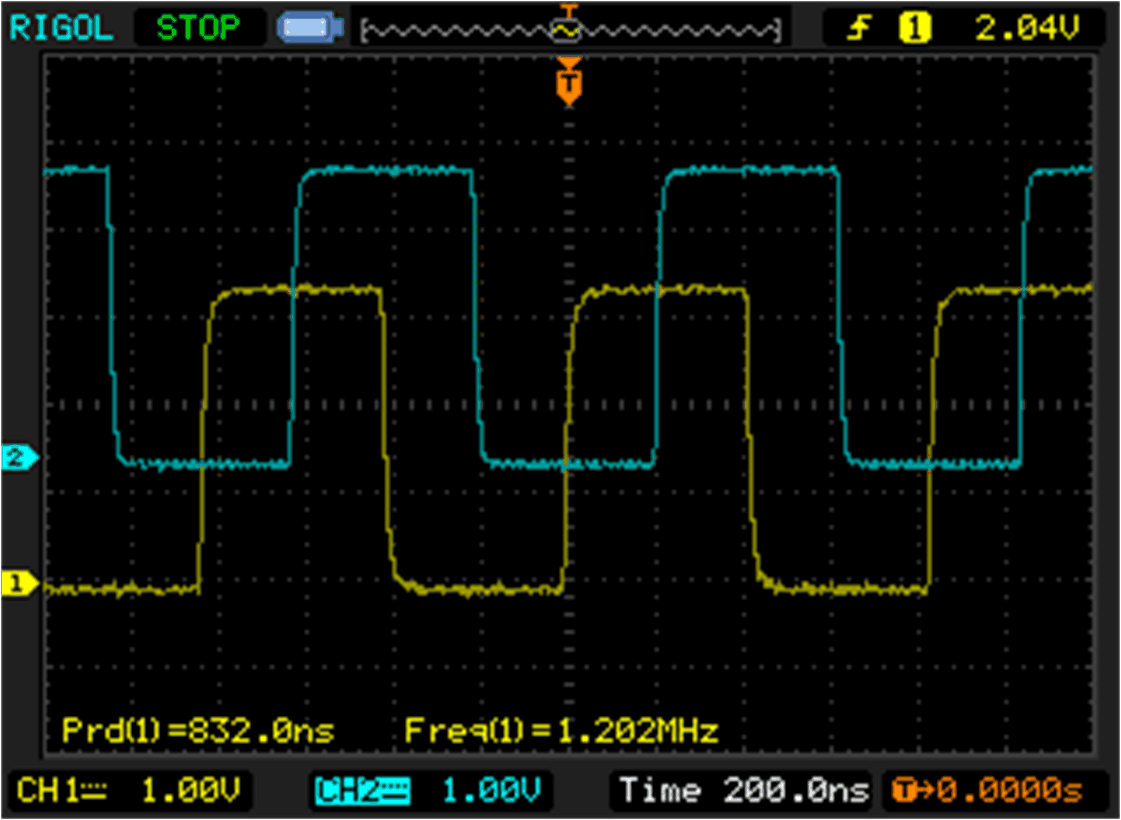
For F28003x, SYSCLK is set to 120 MHz. With a clock divider of 100, the frequency of the generated CLKOUT0_DCLK and CLKOUT1_DCLK are 1.2 MHz. The clock offset of 25 for CLKOUT1_DCLK, offsets the signal from CLKOUT0_DCLK by 200 ns.
If the SIGGEN0 module is configured for any mode other than BIT-BANG mode, the clock generation will stop until the SIGGEN0 module starts a ROTATE or SHIFT. Therefore, inserting the line below will disable the clock generation in this example.
EPG_setSignalGenMode(EPG1_BASE, EPG_SIGGEN0, EPG_SIGGEN_MODE_SHIFT_RIGHT_ONCE);C2000Ware example 7 showcases this example configuration.
 Figure 2-2 Two Offset Clocks