SLYY205A March 2021 – October 2022 TPS562211 , TPS562212 , TPS562231 , TPS563211 , TPS563212 , TPS563231 , TPS56339
PCM
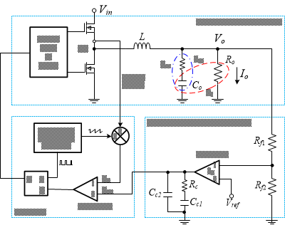
PCM is a popular fixed-frequency control topology for DC/DC converters given its overload protection, accuracy and ease of compensation. Figure 1 iillustrates PCM control of a buck converter
 Figure 1 PCM control scheme block
diagram.
Figure 1 PCM control scheme block
diagram.The power stage consists of the power switches and output filter. The compensation block includes the output voltage divider network, error amplifier, reference voltage and compensation components. The pulse-width modulator uses a comparator to compare the inductor current information with the slope compensation ramp to the error signal, creating an output pulse-train that has a width controllable by the level of the error signal.
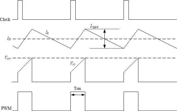
As shown in Figure 2, the internal clock initiates one pulse, and the high-side field-effect transistor (FET) turns on, with current increasing in the inductor. When the sensed current reaches the control voltage, the high-side FET turns off and the low-side FET turns on until the next rising edge of the clock. The next PWM pulse is generated at the next clock pulse. Thus, the switching frequency depending on the clock is truly fixed.
 Figure 2 PCM control scheme
waveform.
Figure 2 PCM control scheme
waveform.PCM control introduces one inner current loop, which transforms the inductor into a voltage-controlled current source. The power stage can be approximated as a current source feeding the parallel combination of the output capacitor and the load resistor, and produces a single low-frequency pole. The power stage also consists of a higher-frequency zero set by the output capacitor and its equivalent series resistance (ESR). Type-II compensation normally introduces one zero and one pole to compensate the output pole and output zero.
Engineers designing with traditional PCM control devices prefer external compensation to achieve good loop performance for wide output-voltage- range applications. However, external compensation complicates loop design and requires more external components. To simplify the design, a growing number of integrated circuit (IC) manufacturers have developed internally compensated PCM control devices that integrate Type-II loop compensation with Rc, Cc1 and Cc2. Rc and Cc1 generate a fixed internal zero to compensate the output pole, while Rc and Cc2 produce a fixed internal high-frequency pole to compensate the output zero. Both the effective output capacitance and load resistance have an impact on the output pole, however. In order to support a wide output-voltage range or wide output-capacitance range, you must set the fixed internal zero relatively low to get good stability. What’s more, the cross-frequency (fc) of PCM control is designed to meet fsw/10 < fc < fsw/5. Therefore, the error amplifier introduces some delay, which limits the load-transient response.
PCM also has these drawbacks:
- The lower the output voltage, the lower the load resistance under a certain output current. Getting the output pole close to the fixed internal zero requires a large output capacitance, resulting in a higher bill-of-materials cost.
- Some PCM devices that clamp the control voltage to achieve high efficiency at a light load may face multipulse issues, resulting in a large output ripple.