SLYY205A March 2021 – October 2022 TPS562211 , TPS562212 , TPS562231 , TPS563211 , TPS563212 , TPS563231 , TPS56339
D-CAP2 control scheme
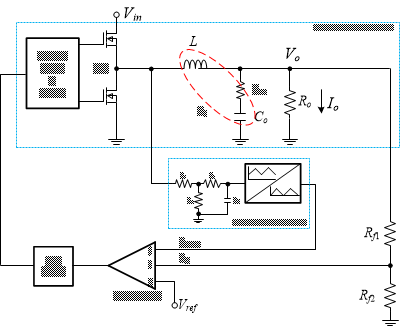
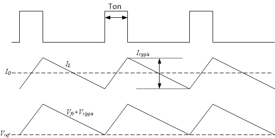
The D-CAP2 control scheme is a variation of adaptive COT control with an emulated ramp-generator circuit integrated inside the IC. This control scheme is popular in buck converters because of its simplicity and improved load-transient performance. Figure 3 shows the block diagram for D-CAP2 control of buck converters, while Figure 4 shows the corresponding control waveforms.
The ramp generator (ripple injection generator) emulates the inductor current information and brings this information back to the comparator. When the emulated ramp voltage and feedback voltage are lower than the reference voltage, the comparator output goes high to initiate an on-time pulse. The width of the on-time pulse (Ton) is constant, since it is calculated by the adaptive on-time generator based on the input voltage, output voltage, output current and frequency setting. The off-time relies on the voltage ripple, which has some variation during a line or load transient. As a result, the switching frequency is pseudo-fixed. During the on-time, the high-side FET turns on and the inductor current increases to charge the output voltage. After the on-time, the high-side FET turns off and the low-side FET turns on. The output voltage goes down until the generation of the next on-time pulse. Because D-CAP2 control topology does not integrate an oscillator or clock, the on-time may be affected by a propagation delay from logic to driver, resulting in poor jitter performance. That is the main reason why it is not easy for IC manufacturers to design high-switching-frequency buck converters (2.1 MHz) with D-CAP2 control topology. Additionally, there are different offset voltages of the emulated ramp-generation circuit under different load conditions, resulting in poor output-voltage accuracy.
 Figure 3 D-CAP2™ control scheme block
diagram.
 Figure 4 D-CAP2 control scheme
waveform.
Figure 4 D-CAP2 control scheme
waveform.The D-CAP control topology requires some ripple on the output where low ESR capacitors can become a problem. That’s why engineers need D-CAP2 control. There is some limitation to the internal emulated ramp-generator circuit of the D-CAP2 buck converter as well, so the traditional D-CAP2 buck converter can only support an output up to 7 V. There is a minimum off-time requirement as well because of the valley voltage detection; thus, D-CAP2 control is not recommended for large duty-cycle applications.
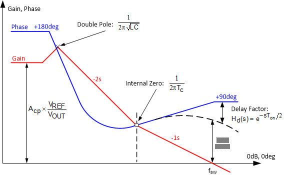
Reference [2] proposed an open-loop transfer function of the D-CAP2 control topology. Figure 5 shows the corresponding Bode plot. The emulated ramp-generation block introduces one internal zero, which can eliminate the double pole set by the output inductor and capacitor, thus making the gain plot crossing the horizontal line 0 dB with a slope of –20 dB per decade, and boosting the phase margin at the crossing frequency. Equation 1 expresses the DC gain of the open-loop transfer as:
where,
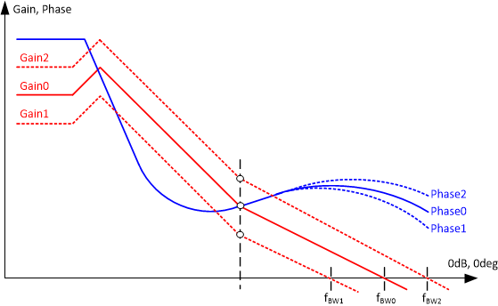
Since Acp and Vref are constant, the DC gain is an inverse proportional of VOUT. As shown in Figure 5, if VOUT1 > VOUT0 > VOUT2, then the DC gain trend is Gain1 < Gain0 < Gain2. For a certain device, the internal zero is fixed. Assuming that the double pole for different outputs is the same, the bandwidth trend is fBW1 < fBW0 < fBW2. Therefore, for a D-CAP2 buck converter, a higher output voltage would have a lower bandwidth.
 Figure 5 Bode plot with different VOUT
conditions of a D-CAP2 buck converter.
Figure 5 Bode plot with different VOUT
conditions of a D-CAP2 buck converter.Since Acp and Vref are constant, the DC gain is an inverse proportional of VOUT. As shown in Figure 6, if VOUT1 > VOUT0 > VOUT2, then the DC gain trend is Gain1 < Gain0 < Gain2. For a certain device, the internal zero is fixed. Assuming that the double pole for different outputs is the same, the bandwidth trend is fBW1 < fBW0 < fBW2. Therefore, for a D-CAP2 buck converter, a higher output voltage would have a lower bandwidth.
 Figure 6 Bode plot with different VOUT
conditions of a D-CAP2™ buck converter.
Figure 6 Bode plot with different VOUT
conditions of a D-CAP2™ buck converter.Additionally, because the duty cycle cannot change with COT control, the on-time generator will produce a delay factor in the loop, causing a phase drop at high frequency. A larger duty cycle means a longer on-time, resulting in a bigger phase drop.