SLVUCF4 August 2022
PRODUCTION DATA
4 Load Transient Circuitry
The TPS7H2221EVM contains a sub-circuit which enables the user to test how the TPS7H2221-SEP responds to a load transient. In many cases an electronic load (e-load) will suffice. However, in some scenarios the inducance introduced by the wire leads to an e-load can cause issues that interfere with testing. This problem is resolved through the use of the load transient sub-circuit that is provided on the EVM.
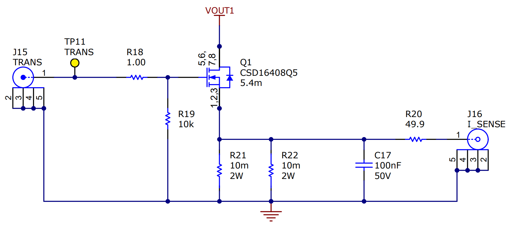
Figure 4-1 shows the schematic for this transient circuit. A power MOSEFT provided by Texas Instruments at Q1 is used to momentarily press the regulated VOUT voltage across power resistors R21 and R22 by modulating the gate of Q1 at JP15 with low duty cycle square wave.
 Figure 4-1 TPS7H2221EVM Load Transient Sub-circuit.
 The default EVM components are configured for output short-circuit testing.
Eliminating the uncertainty of RDSON_Q1 in the calculation of the transient current is possible by capturing the actual voltage at probe testpoint J16 and dividing by (R21||R22).
The key to a successful measurement (i.e. one without a smoking resistor), is to determine the duty cycle to apply to the gate of Q1 to allow the right amount of current through so as to not exceed the power rating of R21 and R22.
R21 and R22 have a power rating of 2 W. The maximum duty cycle of the square wave applied to the gate of Q1 is:
It is a good idea to leaving some margin for error by using a duty cycle lower than the maximum value calculated above.
The resistors on the gate of the FET can be used to control the turn-on and turn-off times of the transient. The voltage amplitude of the low duty cycle square wave applied to the gate of the FET via J15 will also impact the RDSON of the FET.
Output Short-Circuit Testing
If desired, the user is also able to test device behavior under output short-circuit conditions by using low resistances for R21 and R22. This trips the short-circuit protection features of the device, which limit the maximum value of the transient. Faster transients will typically result in higher peak current values.
One must take caution during such tests as they typically exceed the recommended operating conditions of the device, which can lead to damage or degradation of the part.