SLVUC11 April 2021
4 BER Testing
The DP83561EVM supports BER testing through RGMII back-to-back configuration and/or internal loopback modes.
RGMII BER Testing - Back-to-Back Configuration
The DP83561EVM supports RGMII BER testing through back-to-back configuration as described by RGMII Back-to-Back Configuration. BER testing can be conducted using two DP83561EVMs and two link partners by checking the packets sent and received by the two link partners.
Referring to Figure 3-3, should a second link partner, Link Partner B, be unavailable, DP83561EVM B can be programmed into Analog Loopback for the BER test. In this case, Link Partner A will send data across the cable to DP83561EVM A, to be sent across the RGMII interface to DP83561EVM B, looped back to DP83561EVM A, and received by Link Partner A. Please note, that in Analog Loopback, the MDI output pairs must have a 100 ohm differential termination. The RGMII Transmit Clock Delay must be set such that the RGMII transmit clock is aligned with respect to transmit data for both boards. This can be done with the following register write:
- Write Register 0x32 = 0xD2
RGMII BER Testing - External Loopback Configuration
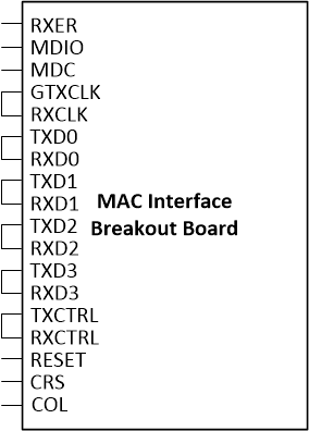
The DP83561EVM support RGMII BER testing through an external loopback configuration using the MAC Interface Breakout Board. The MAC Interface Breakout Board may be connected to the main DP83561EVM board as described in MAC Interface Breakout Board Configuration. To configure the MAC Interface Breakout Board for external loopback, jumpers must be placed to connect the transmit pins to the corresponding receive pins. Refer to Figure 4-1 for a connection diagram. The RGMII Transmit Clock Delay must be set such that the RGMII transmit clock is aligned with respect to transmit data. This can be done with the following register write:
- Write Register 0x32 = 0xD2
 Figure 4-1 MAC Interface Breakout Board External Loopback Connection Diagram
MII BER Testing
In MII mode, the MAC Interface Breakout Board may be used as described in MAC Interface Breakout Board Configuration to support MII BER testing. Referring to Figure 4-2, the link partner, which can be another DP83561EVM, must be configured for Reverse Loopback, and the MII MAC must be configured to generate and receive packets, and check for errors. For additional information on configuring loopback modes, please refer to the device data sheet.
 Figure 4-2 DP83561EVM BER Testing MII Connection Diagram