SLVUAP3A April   2016  – October 2021 TPS54202


  1.   Trademarks
  2. 1Introduction
    1. 1.1 Background
    2. 1.2 Performance Specification Summary
    3. 1.3 Modifications
      1. 1.3.1 Output Voltage Set Point
      2. 1.3.2 Output Capacitor and Feed-Forward Capacitor
      3. 1.3.3 Adjustable UVLO
  3. 2Test Setup and Results
    1. 2.1 Input/Output Connections
    2. 2.2 Efficiency
    3. 2.3 Output Voltage Load Regulation
    4. 2.4 Output Voltage Line Regulation
    5. 2.5 Load Transients
    6. 2.6 Output Voltage Ripple
    7. 2.7 Input Voltage Ripple
    8. 2.8 Powering Up
    9. 2.9 Powering Down
  4. 3Board Layout
    1. 3.1 Layout
  5. 4Schematic and Bill of Materials
    1. 4.1 Schematic
    2. 4.2 Bill of Materials
  6. 5Revision History

Input Voltage Ripple

Figure 2-10 shows the TPS54202EVM-716 input voltage ripple. The output current is the rated full load of
2 A and VIN = 24 V. The ripple voltage is measured directly across the input capacitors.
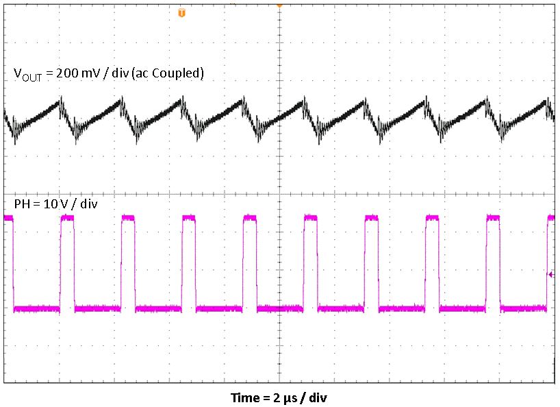
GUID-71C3B663-CB7F-45B8-BB8B-A6410B63BFE5-low.jpgFigure 2-10 TPS54202EVM-716 Input Ripple