SLVUAP3A April   2016  – October 2021 TPS54202


  1.   Trademarks
  2. 1Introduction
    1. 1.1 Background
    2. 1.2 Performance Specification Summary
    3. 1.3 Modifications
      1. 1.3.1 Output Voltage Set Point
      2. 1.3.2 Output Capacitor and Feed-Forward Capacitor
      3. 1.3.3 Adjustable UVLO
  3. 2Test Setup and Results
    1. 2.1 Input/Output Connections
    2. 2.2 Efficiency
    3. 2.3 Output Voltage Load Regulation
    4. 2.4 Output Voltage Line Regulation
    5. 2.5 Load Transients
    6. 2.6 Output Voltage Ripple
    7. 2.7 Input Voltage Ripple
    8. 2.8 Powering Up
    9. 2.9 Powering Down
  4. 3Board Layout
    1. 3.1 Layout
  5. 4Schematic and Bill of Materials
    1. 4.1 Schematic
    2. 4.2 Bill of Materials
  6. 5Revision History

Powering Down

Figure 2-13 and Figure 2-14 show the start-up waveforms for the TPS54202EVM-716. In Figure 2-13, the output voltage ramps down as soon as the input voltage falls below the UVLO stop threshold as set by the R4 and R5 resistor divider network. In Figure 2-14, the output is inhibited by using a 3.3-V logic signal between EN and GND. The input voltage for these plots is 24 V and the load is 5 Ω.
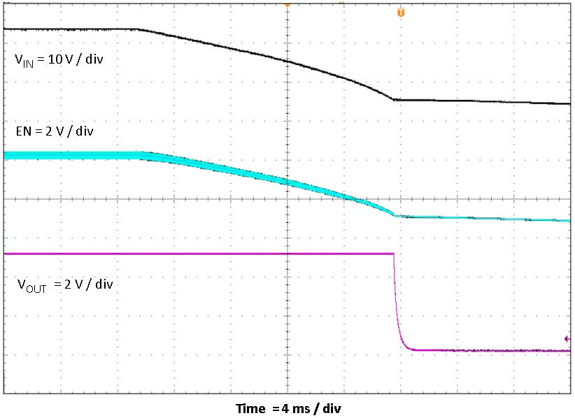
GUID-237943AE-F9FE-4AA3-B27F-C8AE1AB73828-low.jpgFigure 2-13 TPS54202EVM-716 Shutdown Relative to VIN
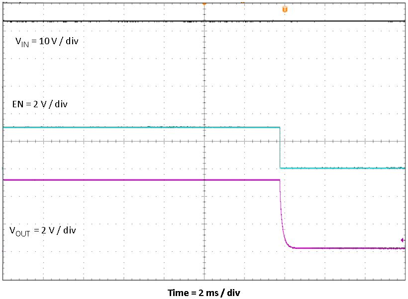
GUID-B102246A-38E8-4B27-B3DA-DA34B02893F2-low.jpgFigure 2-14 TPS54202EVM-716 Shutdown Relative to EN