SLVUA82B November 2014 – June 2021
1.2.2 Loop Response Measurement
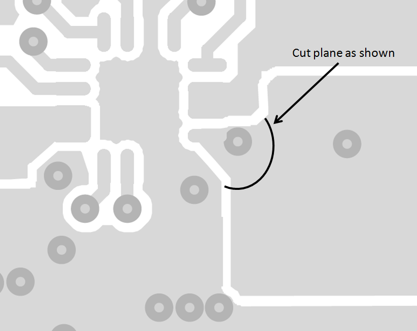
The loop response of the TPS62134xEVM-595 can be measured with two simple changes to the circuitry. First, install a 10-Ω, 0603-sized resistor across the pads of R2 in the middle of the back of the PCB. Second, cut the plane between the via near the VOS pin and the output capacitor C2 and the inductor. This change is shown in Figure 1-1. With these changes, an ac signal (10-mV, peak-to-peak amplitude recommended) can be injected into the control loop across the added resistor. The results of this test are shown in Figure 3-2.
 Figure 1-1 Loop Response Measurement Modification