SLVUA82B November   2014  – June 2021 TPS62134A , TPS62134B , TPS62134C , TPS62134D


  1.   Trademarks
  2. 1Introduction
    1. 1.1 Performance Specification
    2. 1.2 Modifications
      1. 1.2.1 Input and Output Capacitors
      2. 1.2.2 Loop Response Measurement
  3. 2Setup
    1. 2.1 Input/Output Connector Descriptions
    2. 2.2 Setup
  4. 3TPS62134xEVM-595 Test Results
  5. 4Board Layout
  6. 5Schematic and Bill of Materials
    1. 5.1 Schematic
    2. 5.2 Bill of Materials
  7. 6Revision History

Board Layout

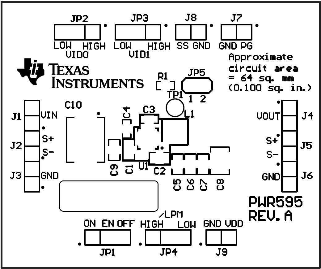
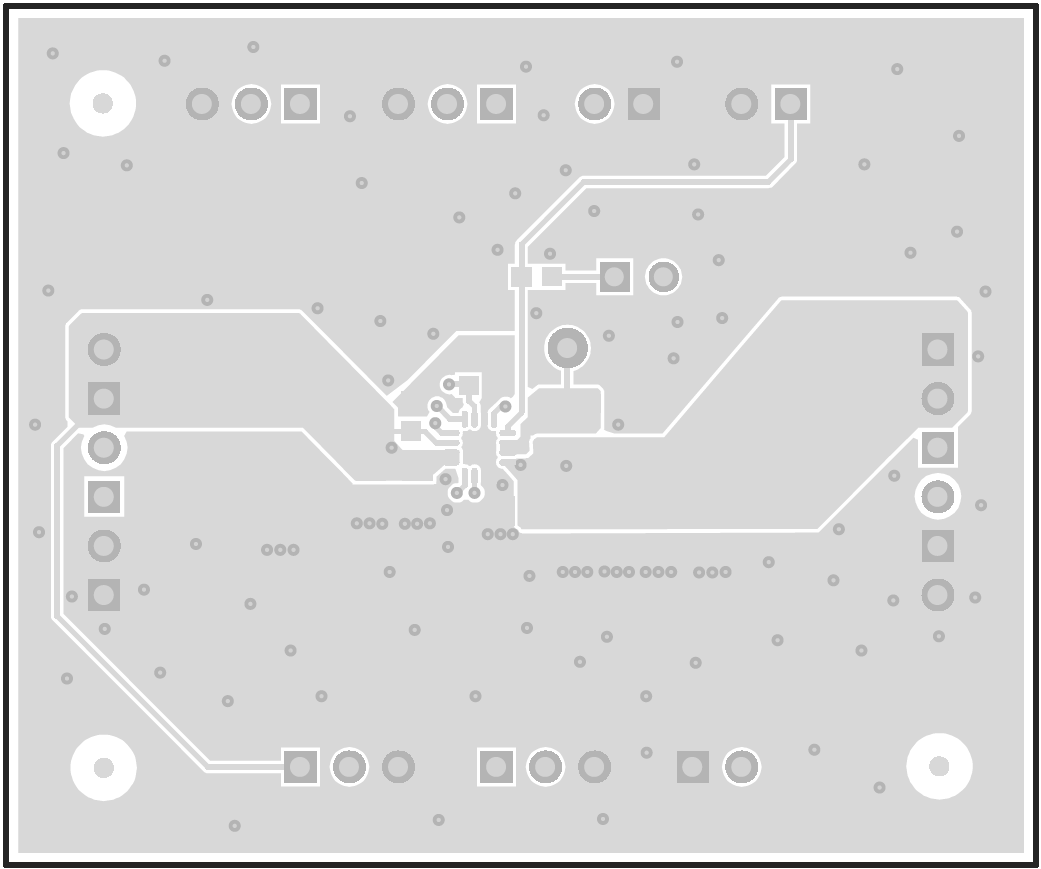
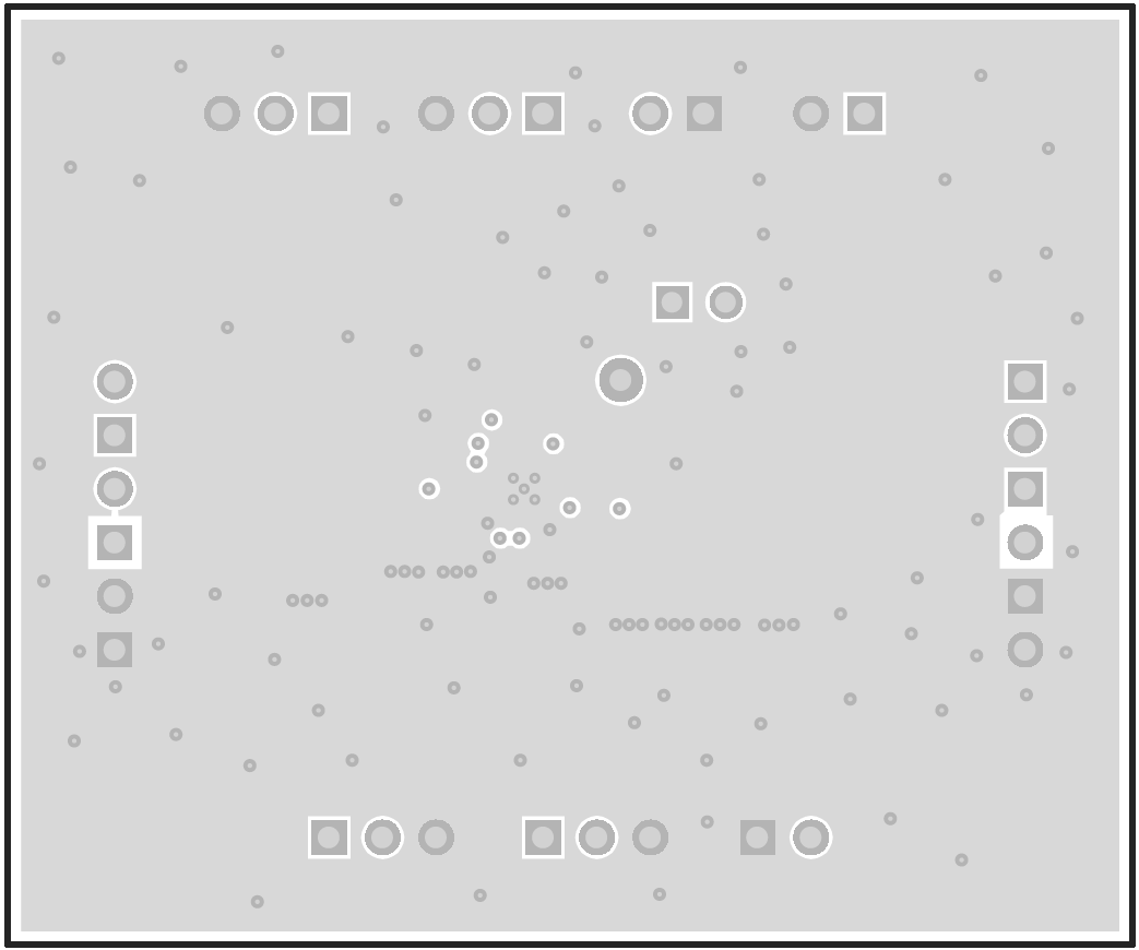
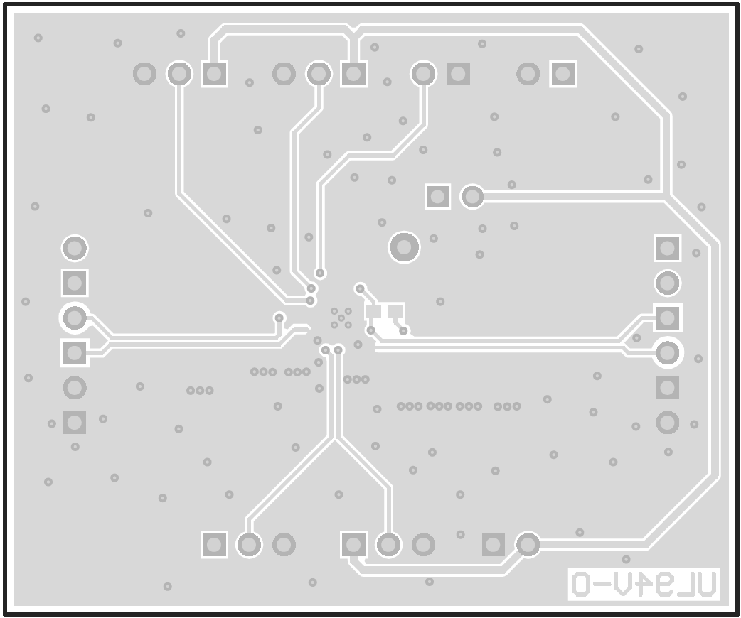
This section provides the TPS62134xEVM-595 board layout and illustrations.
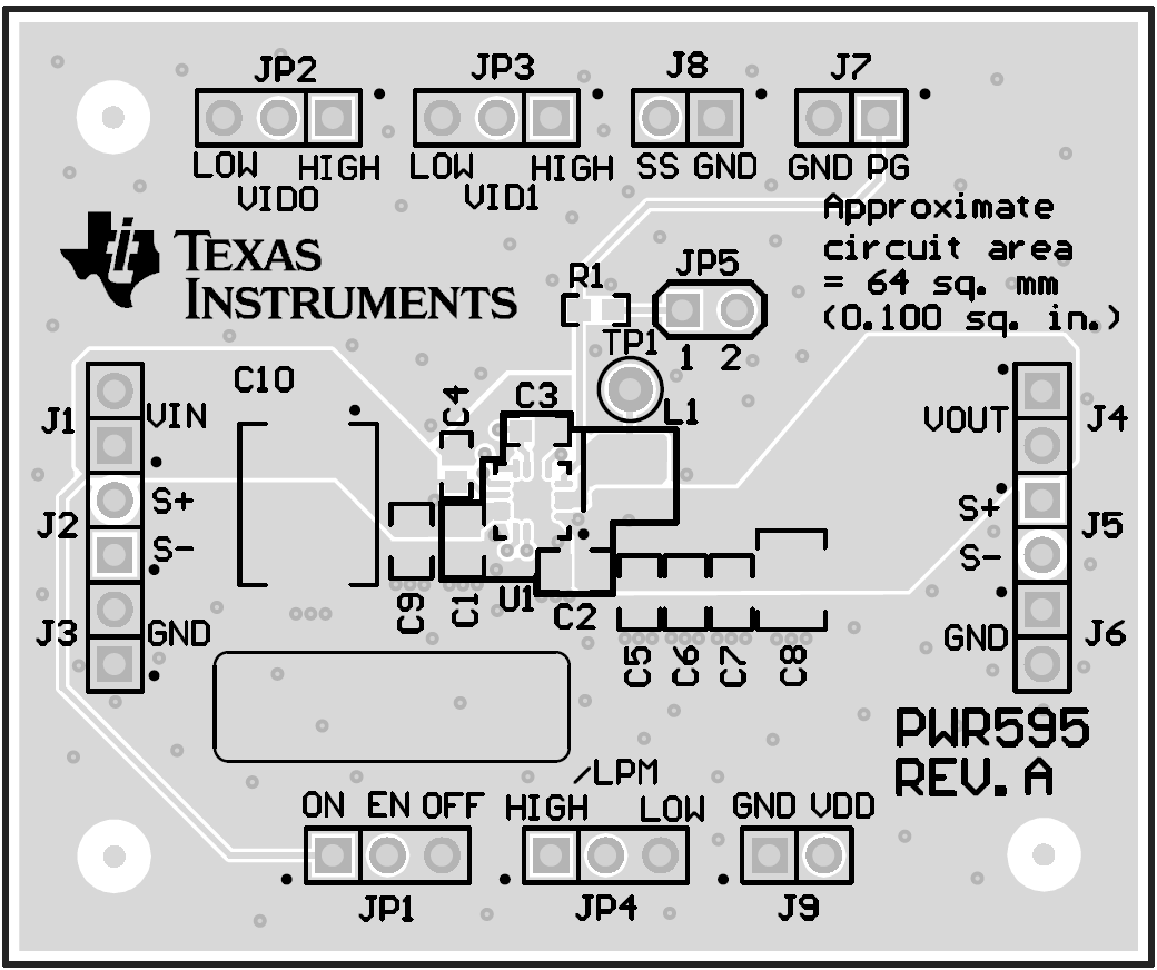
GUID-E1BE473F-42F2-453E-A7EA-A156665F88FC-low.png Figure 4-1 Assembly Layer
GUID-ED034196-BF9B-4423-88A1-674A187260F2-low.png Figure 4-2 Top Silk Layer
GUID-489D9E98-59AC-4571-BF0D-A5D6D09055DD-low.png Figure 4-3 Top Layer
GUID-42896CFA-13AF-4223-8251-7A6520259DEA-low.png Figure 4-4 Internal Layer 1
GUID-04DD1D48-0D5D-42CD-9B0A-0FB02EE2D130-low.png Figure 4-5 Internal Layer 2
GUID-BED24AFB-1545-4754-9C78-52864FF8D281-low.png Figure 4-6 Bottom Layer