SLVAFB4 July 2022 TPS62902-Q1 , TPS62903 , TPS62903-Q1
2.2 MODE/S-CONF Pin
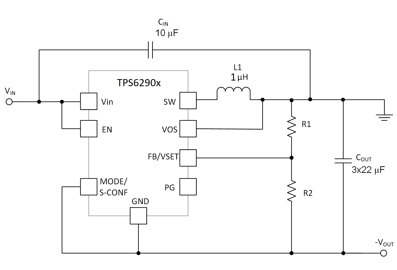
TPS62903 has a MODE/S-CONF pin which can be used to customize the device behavior. Refer to schematic in Figure 2-2 and Figure 2-3
- Selects device configuration (switching frequency, internal or external feedback, output discharge, Forced PWM and Auto PFM/PWM mode) by connecting a single resistor between this pin and -VOUT (IC GND pin) or connecting directly to VIN or -VOUT (IC GND pin).
- A 2.5 MHz switching frequency setting is recommended for inverting buck-boost application due to lower inductor ripple current. The design example selects MODE/S-CONF resistor as 26.1 k which configures internal feedback, 2.5 MHz switching frequency, Auto PFM/PWM with AEE and output discharge enabled.
- Note that the maximum output current will be reduced while using 1uH inductor and 1MHz switching frequency. 2.2uH or larger inductance is strongly recommended for 1 MHz switching frequency configuration, otherwise special care has to be taken to make sure the half ripple current doesn't trip the negative current limit under no load condition.
- Dynamic MODE option is an advance feature which allows MODE/S-CONF pin to actively switch between Forced PWM and Auto PFM/PWM during operation. This feature provides user with the option of controlling when/if the device enters power save mode (DCM). In the inverting buck-boost topology, VIN is HIGH and -VOUT is LOW, but this is only possible by driving the MODE/S-CONF pin between VIN and -VOUT. This can be done with the same type of circuit used to drive the EN pin HIGH and LOW as shown in Figure 2-1
- The external feedback configuration shown in Figure 2-3 , where the MODE/S-CONF pin can be tied to -VOUT directly to configure as 2.5 MHz switching frequency, Auto PFM/PWM with AEE and output discharge enabled.
 Figure 2-3 External Feedback with 2.5 MHz Switching Frequency and Auto PFM/PWM