SLVAEZ7 November 2020 TPS61391
2.1 Schematic Design
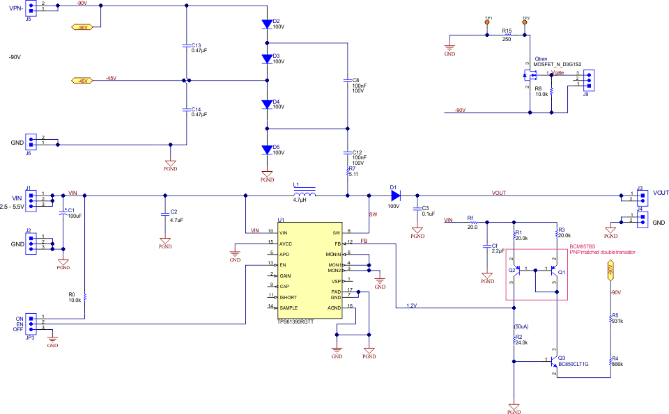
Figure 2-1 shows the schematic of this application note. To achieve -90 V output, two negative charge-pump cells were used. The maximum output voltage of TPS61391 can reach 85 V, so if the required negative voltage is within 0 to -80 V, only one charge pump cell needed; if the required negative voltage is within -80 to -160 V, two charge pump cells should be adopted.
To convert the negative output voltage to a positive feedback voltage, a level shift circuit is implemented. It uses a current mirror circuit built with two inexpensive PNP transistors, and one NPN transistor to regulate the output voltage. For best performance and tighter regulation accuracy, a matched pair can be used, so that the two VBE can be canceled out.
 Figure 2-1 3.3 V Input -90 V Output
Conversion with TPS61391