SLVAEZ7 November 2020 TPS61391
2.2 Parameter Calculation
During normal working, the current IFB flowing through R2 and Q2 equals to Vref/R2. The current flowing through Q1 is effected by the VBE mismatch of Q1 and Q2, but the VBE mismatch can be reduced to a minimum level by using matched double transistors in the design. For the PNP matched double transistors, the VBE mismatch is lower than 2mV, neglect this mismatch, IQ1 can be derived from the below equation:

The output voltage equals to:
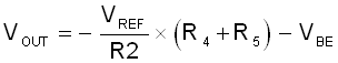
The precision of the output voltage is mainly determined by the tolerance of the output voltage dividing network R2, R4 and R5, the tolerance of the reference voltage Vref and VBE. Set IFB = 50uA, then R2 = 24k ohm based on 1.2 V reference voltage. The value of R1 and R3 is limited by the minimum input voltage, therefore a 20k ohm resistor is chosen in this application note. The total value of R4 and R5 can be calculated by below equation:
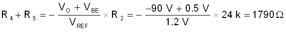
In this application note, the total value of R4 and R5 is set at 1797k ohm, which is quite close to the calculated value.
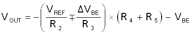
The output voltage drift caused by the VBE mismatch of the PNP matched double transistors Q1 and Q2 can be calculated by the below equations:
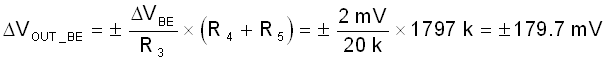
In this application note, BCM857BS is chosen for its <2m V small VBE mismatch.