SLVAEZ7 November 2020 TPS61391
3 Test Result
Figure 3-1 shows the 3.3 V input voltage startup waveform of SLVAEZ7. The output voltage decreases monotonically from 0 V to -90 V.
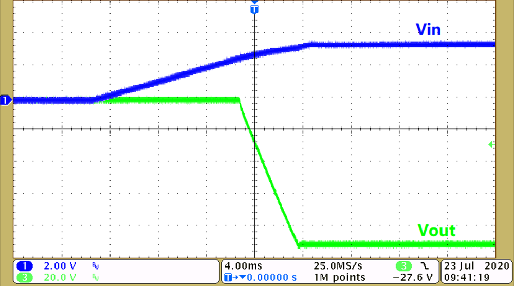 Figure 3-1 Input Voltage Start-up Waveform (Vin=3.3 V,
Vout=-90 V)
Figure 3-1 Input Voltage Start-up Waveform (Vin=3.3 V,
Vout=-90 V)Figure 3-2 shows the enable startup waveform of SLVAEZ7. The output voltage decreases monotonically from 0 V to -90 V.
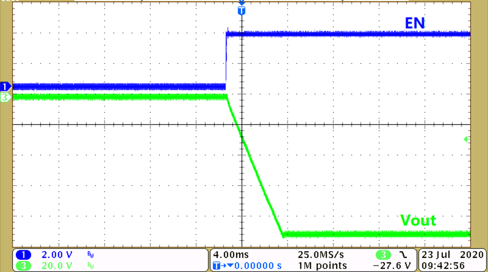 Figure 3-2 Enable Start-up Waveform (Vin=3.3 V,
Vout=-90 V)
Figure 3-2 Enable Start-up Waveform (Vin=3.3 V,
Vout=-90 V)Figure 3-3 and Figure 3-4 show the output voltage ripple at 1mA and 2mA load current respectively. The output voltage ripple is around 20mV at 2mA load current based on schematic show in Figure 2-1.
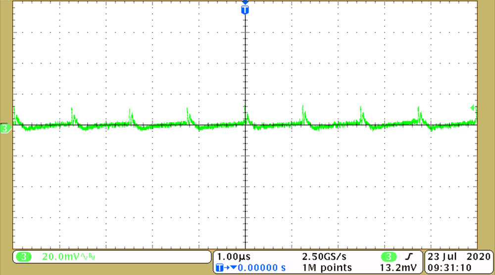 Figure 3-3 Output Voltage Ripple at 1mA load
Current (Vin=3.3 V, Vout=-90 V)
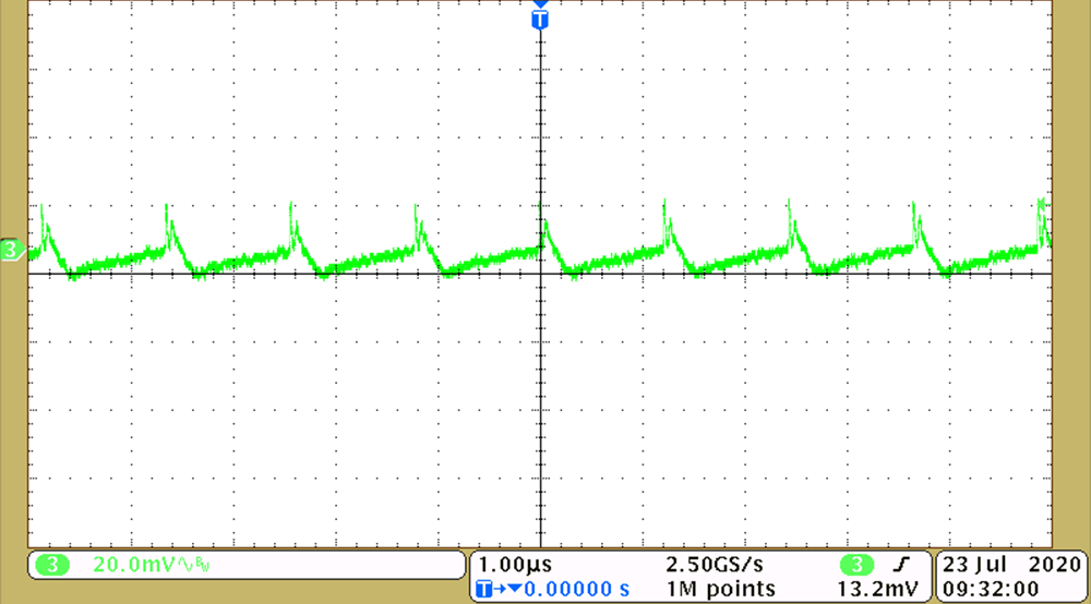 Figure 3-4 Output Voltage Ripple at 2mA load
Current (Vin=3.3 V, Vout=-90 V)
Figure 3-4 Output Voltage Ripple at 2mA load
Current (Vin=3.3 V, Vout=-90 V)Figure 3-5 shows the load dynamic performance. When Vgate high, there’s a current flowing through R15. We control the Vgate high-low level to generate a dynamic load current. The voltage drop on the -90 V output is less than 500mV with a 2mA load step.
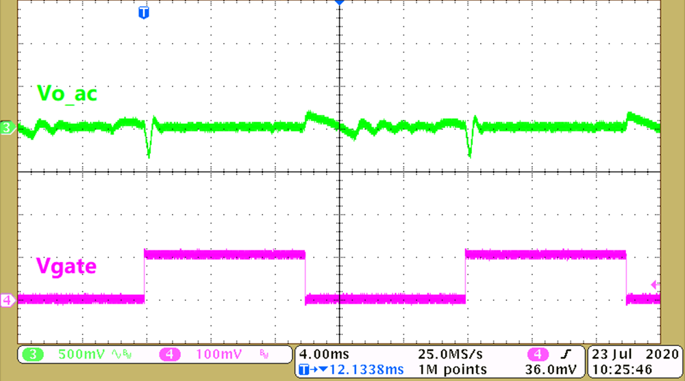 Figure 3-5 Load Dynamic Performance at 2mA Load
Step (Vin=3.3 V, Vout=-90 V)
Figure 3-5 Load Dynamic Performance at 2mA Load
Step (Vin=3.3 V, Vout=-90 V)Table 3-1 shows the line and load regulation performance. The output voltage doesn’t changes with the load, but slightly changes with the input voltage.
| Vin(V) | Vout(V) | ||
|---|---|---|---|
| Io=0mA | Io=1mA | Io=2mA | |
| 3.3 | -90.1 | -90.1 | -90.1 |
| 4 | -90.0 | -90.0 | -90.0 |
| 5 | -89.9 | -89.9 | -89.9 |