SLUP412 February 2022 LMG3522R030-Q1
- 1 Introduction
- 2 Comparing Different Technologies
- 3 Advantages of Integrating the Driver With GaN FETs
- 4 The GaN-Based 6.6-kW OBC Reference Design
- 5 PFC Stage
- 6 DC/DC Stage
- 7 DC/DC Topology Selection
- 8 Frequency Selection
- 9 Core Loss
- 10Loss of ZVS
- 11Dead Time
- 12ISR Bandwidth
- 13Overall
- 14Resonant Tank Design
- 15Thermal Solution
- 16Layout Best Practices
- 17Control-Loop Considerations
- 18Conclusions
- 19References
- 20Important Notice
18 Conclusions
Figure 18-1 shows a picture of the final converter, while Figure 18-2 shows the end-to-end efficiency operating at the highest output current condition. The power density of the design came out at 62.5 W/inch3, or 3.8 kW/L.
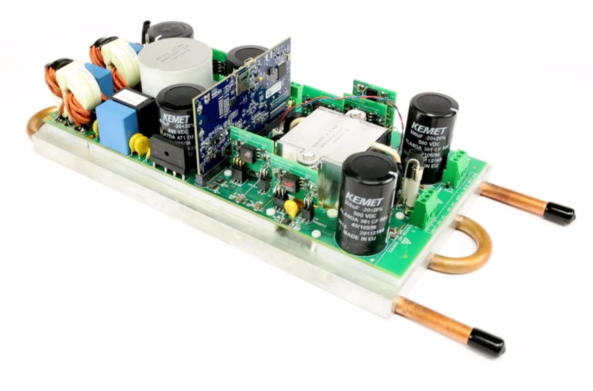 Figure 18-1 6.6-kW OBC with liquid-cooled cold
plate.
Figure 18-1 6.6-kW OBC with liquid-cooled cold
plate.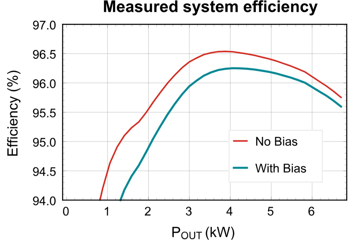 Figure 18-2 Measured system efficiency of the
6.6-kW OBC.
Figure 18-2 Measured system efficiency of the
6.6-kW OBC.GaN’s fast switching performance enables high-frequency power supplies that reduce size while maintaining high efficiency. With these high frequencies, a variety of challenges emerge, requiring cost-effective countermeasures that help maximize the benefits that come from high-speed switching.