SLUAAH3 October 2021 UCC28056
- Trademarks
- 1How to Select the Correct Devices Version of UCC28056 Families?
- 2How to Complete the Schematic Review of the UCC28056?
- 3How to Test and Confirm the UCC28056 Working Mode?
- 4Protections and how to Identify Them?
-
5Application Debug Frequently Asked Questions
(FAQs).
- 5.1 How is the UCC28056 GND Pin Connected?
- 5.2 There is CCM Inductor Current During Start-Up, is This a Normal Phenomenon?
- 5.3 How to Fine-Tune the RC Parameter on the ZCD/CS Pin?
- 5.4 Is it Possible to Increase the High Voltage Cap Value on the ZCD Cap Divider?
- 5.5 How to Separate the TONMAX Limit or OCP Protection When the PFC Output Voltage Cannot Follow the Regulated Voltage?
- 5.6 Does UCC28056 Support DC Input Application?
- 5.7 How Does RDG Change the Delay Time for Valley Switching Detection of the MOSFET?
- 5.8 Can UCC28056 Meet Harmonic Performance?
- 5.9 Does UCC28056 Have Soft Start?
- 5.10 Does the UCC28056 Support Auxiliary-Winding PFC Inductor Input on the ZCD Pin?
- 6References
3.1 How to Capture the ZCD/CS Waveform?
Accurate measurement of the ZCD/CS pin waveform is an important way to fine-tune the robust operation of the UCC28056. To better see what is happening, place the VDS and ZCD/CS pin waveforms on the same scale with the same ground reference, if your oscilloscope allows it. Otherwise, use a 100:1 attenuation probe and a 1:1 probe for the test.
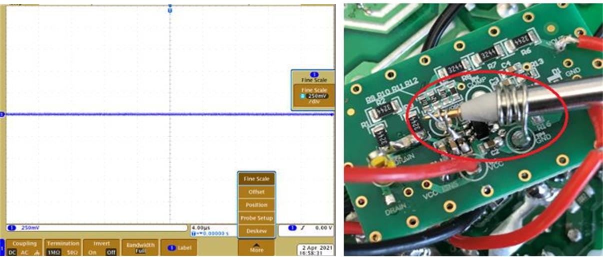
If the VDS waveform is set to 100 V/Div attenuation, click on the ZCD/CS pin channel and select More from the menu. Then select the Fine Scale menu and adjust this channel to 250 mV/Div. The result is 400:1 difference between the scales of the two channels.
Now if the zero line is set at the same point for each channel, the two traces should have the same amplitude.
Since ZCD/CS is sensitive signal, use a low-capacitance probe (below 10 pF) with the smallest test loop between the ZCD/CS pin and ground. Follow Figure 3-1 when setting up the oscilloscope and probe.

Figure 3-1 Fine Scale Menu of the Oscilloscope and Probe Connecting
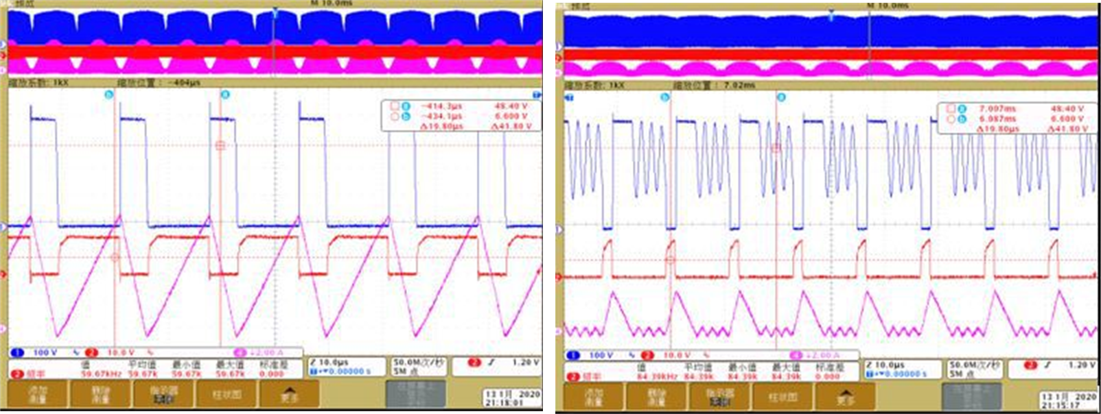
This method allows a clear check of how well these two waveforms are following each other. The waveform in Figure 3-2 shows the VDS and ZCD/CS together.

Figure 3-2 VDS vs ZCD/CS
To achieve a precise sampling of VDS from the ZCD/CS pin, follow the ZCD/CS Pin section in the UCC28056 6-Pin Single-Phase Transition-Mode PFC Controller data sheet to fine tune the amplitude of ZCD/CS to meet VDS.