SLUAAG2 October 2021 UCC28782
4.1 BUR Pin (Programmable Burst Mode)
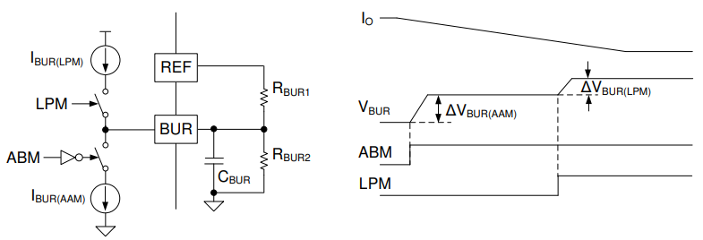
The voltage at the BUR pin (VBUR) sets a target peak current threshold (VCST(BUR)) which programs the onset of adaptive burst mode (ABM) and determines the clamped peak current level of switching cycles in each burst packet. When VBUR is set higher, ABM will start at heavier output load conditions with higher peak current, so the benefit is higher light-load efficiency but the side effect is a larger burst-mode output voltage ripple. Therefore, 50% to 60% of output load at high line is the recommended highest load condition to enter ABM (IO(BUR)) for both Si and GaN-based ACF designs, same as Figure 4-1 showing that IC can program the hysteresis voltage at mode transition.
BUR pin minimum voltage is clamped at 0.7V.
Normally the first high side turn on during the LPM to ABM transition, and it is set by BUR pin, but VDS spike will cause the BIN pin voltage increased during LPM, so deeper burst mode may cause higher voltage then it may damage the BIN and BSW pin, so the BUR pin can set to around 0.7 V as starting point,and then fine tune it during optimizing the average efficiency.
 Figure 4-1 Hysteresis Voltage Generation
on BUR Pin