SLUAAG2 October 2021 UCC28782
4.2 RDM Pin (Sets Synthesized Demagnetization Time for ZVS Tuning)
The RRDM resistor provides the power stage information to the tDM optimizer for auto-tuning the on-time of PWMH to achieve ZVS within a given tz discharge time. The following equation calculates the resistance, based on the knowledge of the primary magnetizing inductance (LM), auxiliary-to-primary turns ratio (NA/NP), the values of the resistor divider (RVS1 and RVS2) from the auxiliary winding to VS pin, and the current sense resistor (RCS). Among those parameters, LM contributes the most variation due to its typically wider tolerance. The optimizer is equipped with wide enough on-time tuning range of PWMH to cover tolerance errors. Therefore, just typical values are enough for the calculation.
The RDM resistance is designed by calculator, and the RDM resistance tuning range is around 30% of calculated result to make sure the internal tuner would not saturate.
Normally the RDM needs to fine tune for SR voltage stress issue.
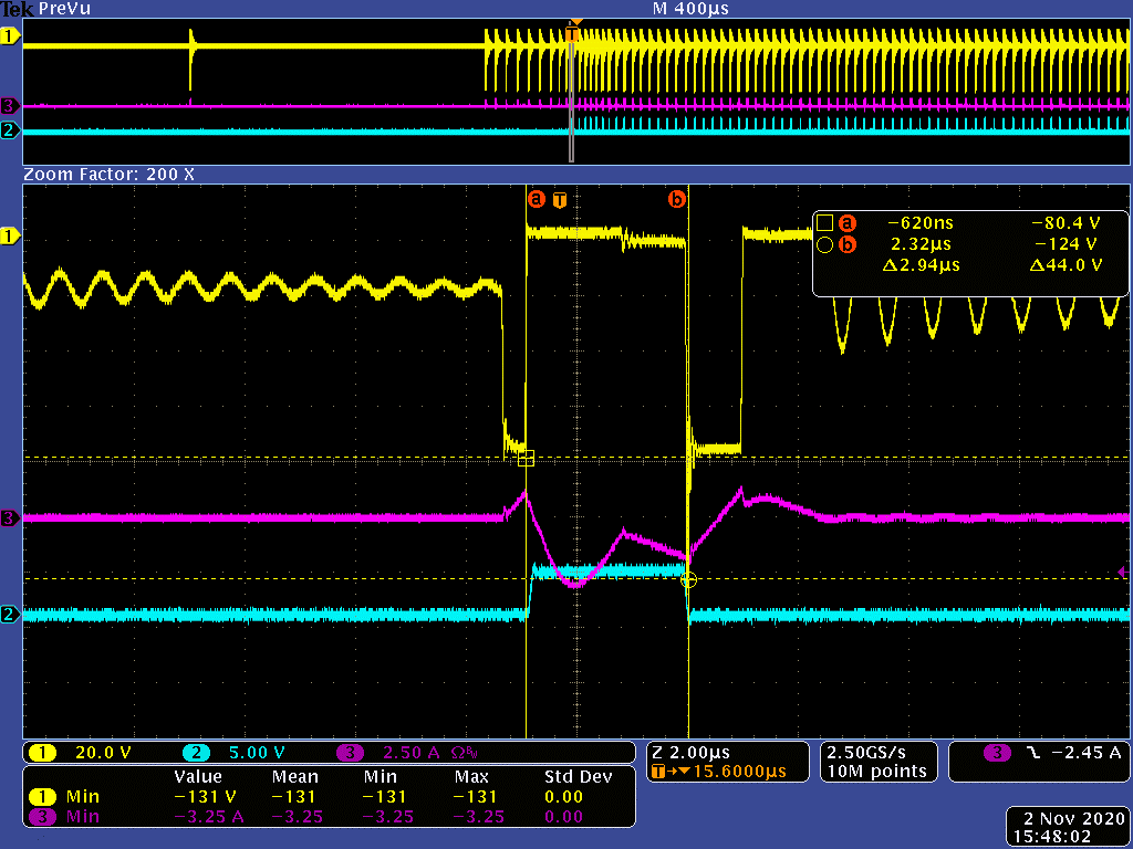
UCC28782 automatically extends the first PWMH pulse width around 140% longer than the following PWMH pulse to prevent it non ZCS turn off. When the high side switch turns off at lower di/dt current instance, the voltage stress can be reduced, but it created more negative magnetizing current, so it would cause SR VDS spike higher as Figure 4-2, so RDM resistance needs to be reduced at this case.
 Figure 4-2 SR VDS spike during first high
side turn on