SLAAE20 May 2021 DAC43701 , DAC43701-Q1 , DAC53701 , DAC53701-Q1
Design Notes
- The DACx3701 10-Bit and 8-Bit, Voltage-Output Smart DACs With Nonvolatile Memory and PMBus™ Compatible I2C Interface With GPI Control Data Sheet recommends using a 100-nF decoupling capacitor for the VDD pin and a 1.5µF or greater bypass capacitor for the CAP pin. The CAP pin is connected to the internal LDO. Place these capacitors close to the device pins.
- An external reference of 1.8V to 5.5V can be applied to the VDD pin of the device. In addition, there is an internal precision 1.21-V reference with ×1.5, ×2, ×3, and ×4 gain options. If using a noisy supply, it is best to use the internal reference instead of VDD as the reference because noise on the reference translates directly to noise on the output of the DAC53701.
- The input signal should not exceed VDD. Also, the maximum threshold voltage is limited by the reference voltage used. If necessary, larger input voltages can be scaled using a voltage divider and the threshold voltage can be adjusted accordingly.
- The GPI_CONFIG field in the CONFIG2 register maps the GPI pin to the various functions.
- To configure a programmable comparator with hysteresis, the GPI will be set to Margin-High, Low function. Set the high threshold in the DAC_MARGIN_HIGH register, and the low threshold in the DAC_MARGIN_LOW register.
- To configure a latching comparator, the GPI pin will be set to Power-Up, Down (10kΩ) function. Set the threshold in the DAC_DATA register.
- Comparator with Hysteresis: In this design, the 5-V VDD supply input is used as the reference. The high threshold value for the comparator is set to is set to 3V using the DAC_MARGIN_HIGH register, and the low threshold is set to 1V using the DAC_MARGIN_LOW register. The codes programmed to these registers, in decimal, is calculated using:
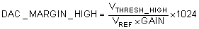

With a 5-V reference, unity gain, and threshold values of 3V and 1V, the equation becomes:


This is rounded to 614d and 205d to give a high threshold of 2.998V and low threshold of 1V.
- Latching Comparator: In this design, the 5-V VDD supply input is used as the reference. The threshold value for the comparator is set to is set to 3V using the DAC_DATA register. The code programmed to this register, in decimal, is calculated using:With a 5-V reference, unity gain, and a threshold value of 3V, the equation becomes:
 This is rounded down to 614d to give a threshold of 2.998V.
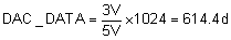
- Using a 5-V reference and the 10-bit DAC53701, the LSB size, or step size between each code, is about 4.88mV. Using lower reference voltages decreases the LSB size and increases the resolution of the threshold value. Using a smaller reference limits the upper limit of the threshold value, but as previously discussed, input voltages can be scaled down if necessary.
- The DAC53701 can be programmed with the initial register settings described in the Register Settings section using I2C. The initial register settings can be saved in the NVM by writing a 1 to the NVM_PROG field of the TRIGGER register. After programming the NVM, the device loads all applicable registers with the values stored in the NVM after a reset or a power cycle.
- The GPI pin starts with a low voltage at start-up due to the pulldown resistor on the output. A high start pulse must be applied to the GPI pin of the latching comparator to power-on the DAC53701. The comparator with hysteresis starts at the low threshold value at start-up.