SLAA558A November 2012 – October 2018 MSP430F5212 , MSP430F5214 , MSP430F5217 , MSP430F5219 , MSP430F5222 , MSP430F5224 , MSP430F5229 , MSP430F5252 , MSP430F5253 , MSP430F5254 , MSP430F5255 , MSP430F5256 , MSP430F5257 , MSP430F5258 , MSP430F5259
- Designing With MSP430F522x and MSP430F521x Devices
- Revision History
7.2 BSL Exit Sequence for DVIO Supplied BSL Interface
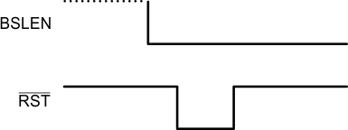
The BSL exit sequence of the DVIO supplied BSL interface involves toggling the RST/NMI pin (high-low-high transition) with the BSLEN pin pulled low (see Figure 4).

A. The minimum timing for this sequence must be within the limits specified for the corresponding pins in the data sheet.
Figure 4. BSL Exit Sequence for DVIO Supplied BSL Interface For complete description of the BSL entry and exit sequences (for both DVCC and DVIO supplied BSL interfaces), features and its implementation, see the MSP430™ Flash Device Bootloader (BSL) User's Guide.