SLAA558A November 2012 – October 2018 MSP430F5212 , MSP430F5214 , MSP430F5217 , MSP430F5219 , MSP430F5222 , MSP430F5224 , MSP430F5229 , MSP430F5252 , MSP430F5253 , MSP430F5254 , MSP430F5255 , MSP430F5256 , MSP430F5257 , MSP430F5258 , MSP430F5259
- Designing With MSP430F522x and MSP430F521x Devices
- Revision History
7.1 BSL Entry Sequence for DVIO Supplied BSL Interface
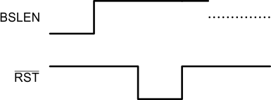
BSLEN is the BSL enable pin with internal pulldown resistor enabled and the BSL entry sequence involves toggling the RST/NMI pin (high-low-high transition) with the BSLEN pin pulled high (see Figure 3).

Note 2:The BSLEN pin need not be pulled high during the entire period when the device is in BSL mode. However, the BSLEN pin is required to be pulled high for a minimum period of time after the RST/NMI pin goes low-high for proper BSL invoke. See the MSP430F522x, MSP430F521x Mixed-Signal Microcontrollers data sheet for the timing specifications.