SLAA351A April 2007 – November 2018 MSP430F2232 , MSP430F2232 , MSP430F2234 , MSP430F2234 , MSP430F2252 , MSP430F2252 , MSP430F2254 , MSP430F2254 , MSP430F2272 , MSP430F2272 , MSP430F2274 , MSP430F2274
3.1 Initialization Routine
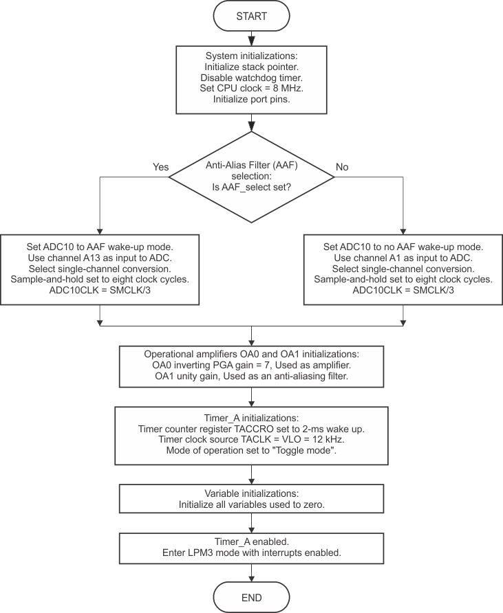
Figure 5 shows a high-level flow diagram of the software execution for initialization of the board. This step occurs at the beginning and after a glass-breakage detect has been issued.
This section of the program initializes all of the peripherals that are needed in the detection routine. The peripherals initialized by this program include Timer_A, CPU clock, ADC10, OAs, and port pins.
The first step is to disable the watchdog timer to avoid an unintended watchdog timer reset. The CPU clock is then set to 8 MHz, and port pins that correspond to the analog inputs are set accordingly. Unused pins are set to outputs, and their values set to high to avoid current consumption. A check on the AAF_select flag is made to enable or disable the AAF. A zero on this flag disables the AAF, and a nonzero value enables it. If this filter is disabled, the input to ADC10 is the output of OA0 and appears at channel A1 of the ADC10. With AAF enabled, the input to ADC10 is the output of OA1, which appears at channel A13 of ADC10. In both cases, the ADC10 is configured with its clock set at SMCLK/3 and for single-conversion mode. Independent of the choice made on the use of AAF, both OA0 and OA1 are configured but not enabled. As mentioned previously, OA0 is configured as an inverting amplifier with a gain of 7 and OA1 as a unity gain buffer. After these initializations are complete, the device enters LPM3, during which time all of the clocks except ACLK (chosen from VLO) are switched off. Timer_A, which is configured to generate an interrupt every 2 ms, wakes the device from this mode.
 Figure 5. Flowchart for Initializations