SLAA126B April   2001  – September 2018 MSP430F149 , MSP430F149 , TLC3544 , TLC3544 , TLC3548 , TLC3548


  1.   Interfacing the TLC3544 or TLC3548 ADC to the MSP430F149 MCU
    1.     Trademarks
    2. 1 Introduction
    3. 2 TLC3544/48 Evaluation Module
    4. 3 Serial Interface
      1. 3.1 Chip Select (CS)
      2. 3.2 Serial Data Input (SDI)
      3. 3.3 Serial Data Output Pin (SDO)
      4. 3.4 Serial Clock Pin (SCLK)
    5. 4 Control and I/O Pins
      1. 4.1 Conversion Start (CSTART)
      2. 4.2 Frame Sync (FS)
      3. 4.3 End of Conversion/Interrupt (EOC/INT)
      4. 4.4 Device Pinout
    6. 5 ADC Initialization and Operation
      1. 5.1 Initializing the ADC
      2. 5.2 Operating the ADC
      3. 5.3 EOC or INT
    7. 6 MSPF149 Code Example
    8. 7 References

EOC or INT

Figure 4 shows the relationship of the EOC and INT signals more clearly. The EOC signal is active low while the ADC is converting the sampled data. It returns to a high state when the conversion is complete.

INT is active low after the (sample plus conversion) period has finished. INT is cleared when a new sample-and-conversion cycle is initiated by either a falling edge of CS (see Figure 4) or rising edge of FS.
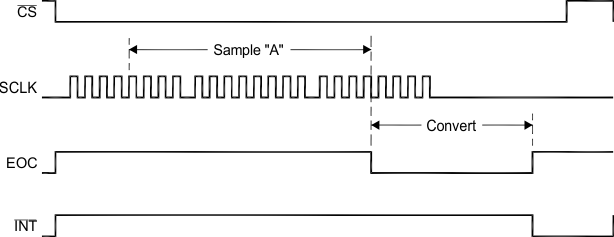
eoc-int-timing.gifFigure 4. EOC/INT Timing