SCDA038 September 2021 TMUX7308F , TMUX7411F , TMUX7412F , TMUX7413F , TMUX7462F
1 Potential Fault Conditions on PLC Analog Input Modules
A list of common, but not exhaustive, fault conditions on the AI Module can be broken down into two broad categories: voltage Electrical Overstress and Latch Up failures. Electrical Overstress can be broken down into four general categories: voltage transients that cause input voltages to go above or below supply rails of the system; an input signal appearing before the system is powered; ground shifting currents which can cause the system to see input voltages beyond supply rails due to differences in ground potential; mis-wiring can cause unexpected voltage rails and/or signal inputs to appear at the front end of the system which could cause inputs being beyond the power rails. While Electrical Overstress and Latch-Up do have some commonalities between them; these events will be examined individually.
The first case to examine is that of Electrical Overstress – focusing on transient signals causing either an undervoltage event or overvoltage event. The causes of voltage transients vary, but transients are common in harsh industrial environments. If the input system includes ESD diodes, example shown in Figure 1-1, a voltage transient can cause one of the diodes to become forward biased if the voltage drop across the diode is less than or equal to the diode’s voltage threshold.
 Figure 1-1 Generalized Analog Input Module with Input ESD Diodes Shown
After the diode becomes forward biased, the current through the diode is given by the Shockley Equation shown in Equation 1
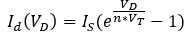
where IS is the saturation current of the diode, VD is the voltage drop across the diode, n is the emission coefficient, and VT is the thermal voltage. The ESD diodes are not designed to handle large sustained currents and with the large currents possible when the voltage ratings are exceeded these diodes are apt to be damaged. When these diodes are damaged they will short either VDD or VSS to the input line depending on the polarity of the transient event.
The next issue that deals with electrical overstress on the system is the case when a signal appears on the input when the system is unpowered. In systems with traditional ESD structures, the input signal wouldn’t have to be that large to cause a diode to become forward biased. While the same issues apply as mentioned with voltage transients during operation – another issue that could show up is that of back-powering. Not only are the ESD diodes subject to damage but the input signal could potentially feed back to any other device on that power rail causing systems to become active prematurely and/or damage systems from having incorrect supplies on more sensitive components. Figure 1-2 shows a simplified analog input module with 2 input sources, a 2:1 multiplexer, an amplifier, and an ADC. The system is unpowered. The red lines represent VDD connections, blue lines for signal pathway, and black lines for VSS connections.
 Figure 1-2 Simplified ASC for Analog Input Module with Front End Multiplexer that has ESD Diode Connections to Power Rails
For a quick example, assume the system power is off, the diodes have a threshold voltage of 0.5 V, IN1 has a signal of 5 V, and IN2 has a signal of -6V . This will cause the diodes from VDD to IN1 to become forward biased while creating a VDD voltage of 4.5 V (input – diode drop). While the diodes on the second input will be forward biased from VSS to IN2 and creating a VSS voltage of -4.5 V (input + diode drop). Now both the amp and ADC have voltages on their power rails, which can cause unexpected operation and potential damage.
The next issue, ground shifting, is a bit more complex. In PLC systems many different components are going to be directly connected via a ground pin or indirectly for devices with no ground pin as the devices power supplies are still referenced to a ground node. With many potential devices return current pathway emptying into this node, ground reference points can be shifted causing different ground nodes to be at different voltages w.r.t. to the input power’s ground connection. The reason why this happens can be explained by looking at the ideal case of a system – see Figure 1-3 – versus the real version of the system – see Figure 1-4.
 Figure 1-3 Ideal Generalized System Diagram
 Figure 1-4 Generalized System Diagram with Trace
Resistance Shown
Figure 1-4 Generalized System Diagram with Trace
Resistance ShownFrom the previous two images it can be shown that the ideal case (Figure 1-3) has no impedance between different ground connections. This is not technically true due to the fact that even the low impedance ground trace / ground plane still is not 0 ohms, but it is low. However, in certain industrial and automotive applications this small impedance in the ground plane starts to make a difference. If the return current running through ground is high enough, the ground connection points can be lifted above ground. For example, imagine Iout2 is 3 A and all the other currents are << 3 A and all the resistances are equal to 0.2 Ohms. This will create ground references that are not equal to zero volts with respect to the system ground which can cause input signals to be outside of the operating range of the device which can lead to system damage. Table 1-1 shows the new ground potentials with the above example.
| Device / Source | Ground Potential (w.r.t. VDD’s Ground) |
|---|---|
| VDD | 0 V |
| Vin_1 | 0.6 V |
| Sub-System1 | 1.2 V |
| Sub-System2 | 1.8 V |
| Vout1 | 2.4 V |
| Vin_2 | 3.0 V |
| Sub-System3 | 3.6 V |
| Vout2 | 4.2 V |
At first glance this may not seem like a large problem, but these shifts can cause the subsystems to become out of spec. Assume that VDD = Vin_1 = Vin_2 = 44V, and look to Table 1-1, Table 1-2, Table 1-3. and Table 1-4 to see the issues that are possible from ground shifting, for simplicity the output voltages have been ignored for this specific example. All voltages shown are with respect to system ground, which is located at the negative terminal of VDD in this example.
| Device/Source | Nominal Voltage | Ground Shift | New Max | New Ground |
|---|---|---|---|---|
| VDD | 44 V | 0 V | 44 V | 0 V |
| Vin_1 | 44 V | 0.6 V | 44.6 V | 0.6 V |
| Vin_2 | 44 V | 3.0 V | 47 V | 3.0 V |
| Sub-System | Upper Limit | Lower Limit After Ground Shift |
|---|---|---|
| Sub-System1 | 44 V | 1.2 V |
| Sub-System2 | 44 V | 1.8 V |
| Sub-System3 | 44 V | 3.6 V |
| Sub-System1 Undervoltage | Sub-System1 Overvoltage | Sub-System2 Undervoltage | Sub-System2 Overvoltage | Sub-System3 Undervoltage | Sub-System3 Overvoltage | |
|---|---|---|---|---|---|---|
| Vin_1 | Yes 0.6 V < 1.2 V | Yes 44.6 V > 44 V | Yes 0.6 V < 1.8 V | Yes 44.6 V > 44 V | No No Connection | No No Connection |
| Vin_2 | No No Connection | No No Connection | No No Connection | No No Connection | Yes 3 V < 3.6 V | Yes 47 V > 44 V |
From the previous tables it is shown that the Sub-Systems don’t have an increase in the max voltage that can be accepted but the lowest signal accepted has increased in value. Now when Vin_1 hits its max or min voltage Sub-System1 and potentially Sub-System2 are going to experience overvoltage and/or undervoltage events. The same can be seen with Vin_2 and Sub-System3. During events where a large ground shift is possible the signal chain can experience electrical overstress and therefore erroneous results and/or system damage.
The final broad category of electrical overstress has to deal with miswiring. When the input of a system is miswired the biggest concern is potential electrical overstress. This can occur due to connecting a power supply to an input, or connecting an input to a pin/port that isn’t able to handle the prescribed voltage. These human mistakes when prepping systems can cause electrical overstress which ultimately can damage/destroy the system.
While the other issues all dealt directly with electrical overstress there is one more outlier than can be disastrous for system designers – this is CMOS Latch Up. Latch up failures occur when VDD is shunted to VSS/GND and the issue doesn’t resolve until the power is cycled or system failure occurs. The cause of latch up is a parasitic silicon-controlled rectifier (SCR) that exists in traditional CMOS manufacturing processes. The SCR is shown in Figure 1-5 – analyzing this circuit gives intuition on how failure occurs.
 Figure 1-5 Parasitic SCR Equivalent Circuit
Examining the SCR, two potential fail scenarios are shown – an injected current or a signal that is greater than VDD or less VSS/GND will cause the BJT’s to conduct. However, there is one other and that is a fast transient can also cause the BJT’s to conduct and trigger a latch-up event – these are often referred to as transient induced latch-up. This poses a serious risk to the system. If any of the three main causes of latch up exist on the input of a system that is vulnerable to latch-up events the device will shunt VDD to VSS/GND. This process will not only potentially damage the IC experiencing the latch-up, but can cause the power rails to sag potentially damaging more sensitive components on the signal chain.
These fail categories provide an insight to failure mechanisms of Analog Input Systems used in a PLC. These issues must be overcome to have reliable and accurate operation of the PLC which is critical in industrial applications. In the past this has been done in a variety of ways including discrete components; however, in many situations the most optimal solution for cost, solution size, and performance is to integrate protection features into the first elements of the analog input system – the analog switch/multiplexer.