SBOS407D December 2007 – May 2016 VCA821
PRODUCTION DATA.
- 1 Features
- 2 Applications
- 3 Description
- 4 Revision History
- 5 Device Comparison Table
- 6 Pin Configuration and Functions
-
7 Specifications
- 7.1 Absolute Maximum Ratings
- 7.2 ESD Ratings
- 7.3 Recommended Operating Conditions
- 7.4 Thermal Information
- 7.5 Electrical Characteristics: VS = ±5 V
- 7.6 Typical Characteristics: VS = ±5 V, DC Parameters
- 7.7 Typical Characteristics: VS = ±5 V, DC and Power-Supply Parameters
- 7.8 Typical Characteristics: VS = ±5 V, AVMAX = 6 dB
- 7.9 Typical Characteristics: VS = ±5 V, AVMAX = 20 dB
- 7.10 Typical Characteristics: VS = ±5 V, AVMAX = 32 dB
- 8 Parameter Measurement Information
- 9 Detailed Description
- 10Application and Implementation
- 11Power Supply Recommendations
- 12Layout
- 13Device and Documentation Support
- 14Mechanical, Packaging, and Orderable Information
9 Detailed Description
9.1 Overview
The VCA821 is a voltage controlled variable gain amplifier with differential inputs and a single ended output. The maximum gain is set by external resistors while the gain range is controlled by an external analog voltage. The maximum gain is designed for gains of 2 V/V up to 100 V/V and the analog control allows a gain range of over 40 dB. The VCA821 Input consists of two buffers which, together create a fully symmetrical, high impedance differential input with a typical common mode rejection of 80 dB. The gain set resistor is connected between the two input buffer output pins, so that the input impedance is independent of the gain settings. The bipolar inputs have a input voltage range of +1.6 V and –2.1 V on ±5 V supplies. The amplifier maximum gain is set by external resistors, but the internal gain control circuit is controlled by a continuously variable, analog voltage. The gain control is a multiplier stage which is linear in dB. The gain control input pin operates over a voltage range of 0 V to 2 V. The VCA821 contains a high speed, high current output buffer. The output stage can typically swing ±3.9 V and source/sink ±90 mA. The VCA821 can be operated over a voltage range of ±3.5 V to ±6 V.
9.2 Feature Description
The VCA821 can be operated with both single ended or differential input signals. The inputs present consistently high impedance across all gain configurations. By using an analog control signal the amplifier gain is continuously variable for smooth, glitch free gain changes. With a large signal bandwidth of 320 MHz and a slew rate of 2500 V/us the VCA821 offers linear performance over a wide range of signal amplitudes and gain settings. The low impedance/high current output buffer can drive loads ranging from low impedance transmission lines to high-impedance, switched-capacitor analog to digital converters. By using closely matched internal components the VCA821 offers gain accuracy of ±0.3 dB.
9.3 Device Functional Modes
The VCA821 functions as a differential input, single-ended output variable gain amplifier. This functional mode is enabled by applying power to the amplifier supply pins and is disabled by turning the power off.
The gain is continuously variable through the analog gain control input. While the gain range is fixed the maximum gain is set by two external components, Rf and Rg as shown in the Figure 73. The maximum gain is equal to 2x (Rf / Rg). This gain is achieved with a 2-V voltage on the gain adjust pin VG. As the voltage decreases on the VG pin, the gain decreases in a linear in dB fashion with over 40 dB of gain range from 2-V to 0-V control voltage.
As with most other differential input amplifiers, inputs can be applied to either one or both of the amplifier inputs. The amplifier gain is controlled through the gain control pin.
9.3.1 Maximum Gain of Operation
This section describes the use of the VCA821 device in a fixed-gain application in which the VG control pin is set at VG = +1 V. The tradeoffs described here are with bandwidth, gain, and output voltage range.
In the case of an application that does not make use of the VGAIN but requires some other characteristic of the VCA821 device, the RG resistor must be set so that the maximum current flowing through the resistance IRG is less than ±2.6 mA typical, or 5.2 mAPP as defined in the Electrical Characteristics table and must follow Equation 1.

As Equation 1 illustrates, when the output dynamic range and maximum gain are defined, the gain resistor is set. This gain setting in turn affects the bandwidth because to achieve the gain (and with a set gain element), the feedback element of the output stage amplifier is set as well. Keeping in mind that the output amplifier of the VCA821 device is a current-feedback amplifier, the larger the feedback element, the lower the bandwidth because the feedback resistor is the compensation element.
Limiting the discussion to the input voltage only and ignoring the output voltage and gain, Figure 1 illustrates the tradeoff between the input voltage and the current flowing through the gain resistor.
9.3.2 Output Current and Voltage
The VCA821 device provides output voltage and current capabilities that are unsurpassed in a low-cost monolithic VCA. Under no-load conditions at +25°C, the output voltage typically swings closer than 1 V to either supply rails; the +25°C swing limit is within 1.2 V of either rails. Into a 15-Ω load (the minimum tested load), it is tested to deliver more than ±90 mA.
The specifications described above, though familiar in the industry, consider voltage and current limits separately. In many applications, it is the voltage × current, or V-I product, that is more relevant to circuit operation. Refer to the Output Voltage and Current Limitations plot (Figure 47) in the Typical Characteristics: VS = ±5 V, AVMAX = 20 dB. The X- and Y-axes of this graph show the zero-voltage output current limit and the zero-current output voltage limit, respectively. The four quadrants give a more detailed view of the VCA821 device output drive capabilities, noting that the graph is bounded by a aafe operating area of 1-W maximum internal power dissipation. Superimposing resistor load lines onto the plot shows that the VCA821 device can drive ±2.5 V into 25 Ω or ±3.5 V into 50 Ω without exceeding the output capabilities or the 1-W dissipation limit. A 100-Ω load line (the standard test circuit load) shows the full ±3.9-V output swing capability, as shown in the Typical Characteristics.
The minimum specified output voltage and current over-temperature are set by worst-case simulations at the cold temperature extreme. Only at cold startup do the output current and voltage decrease to the numbers shown in the Electrical Characteristics table. As the output transistors deliver power, the respective junction temperatures increase, thereby increasing the available output voltage swing and output current.
In steady-state operation, the available output voltage and current are always greater than the temperature shown in the over-temperature specifications because the output stage junction temperatures are higher than the specified operating ambient.
9.3.3 Input Voltage Dynamic Range
The VCA821 device has a input dynamic range limited to +1.6 V and –2.1 V. Increasing the input voltage dynamic range can be done by using an attenuator network on the input. If the VCA821 device is trying to regulate the amplitude at the output, such as in an AGC application, the input voltage dynamic range is directly proportional to Equation 2.

As such, for unity-gain or under-attenuated conditions, the input voltage must be limited to the CMIR of ±1.6 V (3.2VPP) and the current (IRQ) must flow through the gain resistor, ±2.6 mA (5.2mAPP). This configuration sets a minimum value for RE such that the gain resistor must be greater than Equation 3.

Values lower than 615.4 Ω are gain elements that result in reduced input range, as the dynamic input range is limited by the current flowing through the gain resistor RG (IRG). If the IRG current limits the performance of the circuit, the input stage of the VCA821 device goes into overdrive, resulting in limited output voltage range. Such IRG-limited overdrive conditions are shown in Figure 49 for the gain of 20 dB and Figure 69 for the 32-dB gain.
9.3.4 Output Voltage Dynamic Range
With its large output current capability and its wide output voltage swing of ±3.9-V typical on 100-Ω load, it is easy to forget other types of limitations that the VCA821 device can encounter. For these limitations, careful analysis must be done to avoid input stage limitation: either voltage or IRG current.
NOTE
If control pin VG varies, the gain limitation may affect other aspects of the circuit.
9.3.5 Bandwidth
The output stage of the VCA821 device is a wideband current-feedback amplifier. As such, the feedback resistance is the compensation of the last stage. Reducing the feedback element and maintaining the gain constant limits the useful range of IRG, and therefore, reduces the gain adjust range. For a given gain, reducing the gain element limits the maximum achievable output voltage swing.
9.3.6 Offset Adjustment
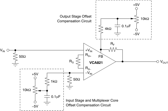
As a result of the internal architecture used on the VCA821 device, the output offset voltage originates from the output stage and from the input stage and multiplier core. Figure 74 shows how to compensate both sources of the output offset voltage. Use this procedure to compensate the output offset voltage: starting with the output stage compensation, set VG = –1 V to eliminate all offset contribution of the input stage and multiplier core. Adjust the output stage offset compensation potentiometer. Finally, set VG = +1 V to the maximum gain and adjust the input stage and multiplier core potentiometer. This procedure effectively eliminates all offset contribution at the maximum gain. Because adjusting the gain modifies the contribution of the input stage and the multiplier core, some residual output offset voltage remains.
 Figure 74. Adjusting the Input and Output Voltage Sources
9.3.7 Noise
The VCA821 device offers 6 nV/√Hz input-referred voltage noise density at a gain of 20 dB and 2.6 pA/√Hz input-referred current noise density. The input-referred voltage noise density considers that all noise terms (except the input current noise but including the thermal noise of both the feedback resistor and the gain resistor) are expressed as one term.
This model is formulated in Equation 4 and Figure 88.

A more complete model is shown in Figure 89. For additional information on this model and the actual modeled noise terms, please contact the High-Speed Product Application Support team at www.ti.com.
9.3.7.1 Input and ESD Protection
The VCA821 device is built using a very high-speed complementary bipolar process. The internal junction breakdown voltages are relatively low for these very small geometry devices. These breakdowns are reflected in the Absolute Maximum Ratings table.
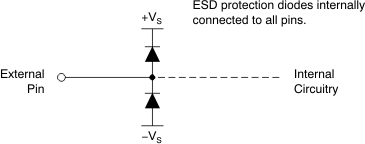
All pins on the VCA821 device are internally protected from ESD by means of a pair of back-to-back reverse-biased diodes to either power supply, as shown in Figure 75. These diodes begin to conduct when the pin voltage exceeds either power supply by about 0.7 V. This situation can occur with loss of the amplifier power supplies while a signal source is still present. The diodes can typically withstand a continuous current of 30 mA without destruction. To ensure long-term reliability, however, diode current should be externally limited to 10 mA whenever possible.
 Figure 75. Internal ESD Protection