SBOS407D December 2007 – May 2016 VCA821
PRODUCTION DATA.
- 1 Features
- 2 Applications
- 3 Description
- 4 Revision History
- 5 Device Comparison Table
- 6 Pin Configuration and Functions
-
7 Specifications
- 7.1 Absolute Maximum Ratings
- 7.2 ESD Ratings
- 7.3 Recommended Operating Conditions
- 7.4 Thermal Information
- 7.5 Electrical Characteristics: VS = ±5 V
- 7.6 Typical Characteristics: VS = ±5 V, DC Parameters
- 7.7 Typical Characteristics: VS = ±5 V, DC and Power-Supply Parameters
- 7.8 Typical Characteristics: VS = ±5 V, AVMAX = 6 dB
- 7.9 Typical Characteristics: VS = ±5 V, AVMAX = 20 dB
- 7.10 Typical Characteristics: VS = ±5 V, AVMAX = 32 dB
- 8 Parameter Measurement Information
- 9 Detailed Description
- 10Application and Implementation
- 11Power Supply Recommendations
- 12Layout
- 13Device and Documentation Support
- 14Mechanical, Packaging, and Orderable Information
10 Application and Implementation
NOTE
Information in the following applications sections is not part of the TI component specification, and TI does not warrant its accuracy or completeness. TI’s customers are responsible for determining suitability of components for their purposes. Customers should validate and test their design implementation to confirm system functionality.
10.1 Application Information
The VCA821 has flexible maximum gain which is set by the Rf and Rg resistors shown in Figure 73. The maximum gain is equal to 2x (Rf / Rg). This gain is achieved with a 2-V voltage on the gain adjust pin VG. As the voltage decreases on the VG pin, the gain decreases in a linear in dB fashion with over 40 dB of gain range from 2-V to 0-V control voltage.
10.1.1 Design-In Tools
10.1.1.1 Demonstration Boards
Two printed circuit boards (PCBs) are available to assist in the initial evaluation of circuit performance using the VCA821 device in the two package options. Both of these are offered free of charge as unpopulated PCBs that are delivered with a user's guide. The summary information for these fixtures is shown in Table 1.
Table 1. EVM Ordering Information
| PRODUCT | PACKAGE | BOARD PART NUMBER | LITERATURE NUMBER |
|---|---|---|---|
| VCA821ID | SOIC-14 | DEM-VCA-SO-1B | SBOU050 |
| VCA821IDGS | VSSOP-10 | DEM-VCA-VSSOP-1A | SBOU051 |
The demonstration fixtures can be requested at the Texas Instruments web site (www.ti.com) through the VCA821 device product folder.
10.1.1.2 Macromodels and Applications Support
Computer simulation of circuit performance using SPICE is often useful when analyzing the performance of analog circuits and systems. This principle is particularly true for video and RF amplifier circuits where parasitic capacitance and inductance can play a major role in circuit performance. A SPICE model for the VCA821 device is available through the TI web page. The applications group is also available for design assistance. The models available from TI predict typical small-signal ac performance, transient steps, DC performance, and noise under a wide variety of operating conditions. The models include the noise terms found in the electrical specifications of the relevant product data sheet.
10.1.1.3 Operating Suggestions
Operating the VCA821 optimally for a specific application requires trade-offs between bandwidth, input dynamic range and the maximum input voltage, the maximum gain of operation and gain, output dynamic range and the maximum input voltage, the package used, loading, and layout and bypass recommendations. The Typical Characteristics have been defined to cover as much ground as possible to describe the VCA821 operation. There are four sections in the Typical Characteristics:
- VS = ±5 V DC Parameters and VS = ±5V DC and Power-Supply Parameters, which include DC operation and the intrinsic limitation of a VCA821 device design
- VS = ±5 V, AVMAX = 6 dB Gain of 6dB Operation
- VS = ±5 V, AVMAX = 20 dB Gain of 20dB Operation
- VS = ±5 V, AVMAX = 32 dB Gain of 32dB Operation
Where the Typical Characteristics describe the actual performance that can be achieved by using the amplifier properly, the following sections describe in detail the trade-offs needed to achieve this level of performance.
10.1.1.4 Package Considerations
The VCA821 device is available in both SOIC-14 and VSSOP-10 packages. Each package has, for the different gains used in the typical characteristics, different values of RF and RG in order to achieve the same performance detailed in the Electrical Characteristics table.
Figure 76 shows a test gain circuit for the VCA821 device. Table 2 lists the recommended configuration for the SOIC-14 and VSSOP-10 packages.
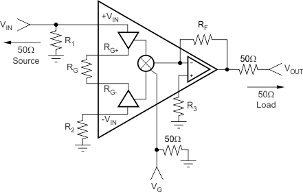 Figure 76. Test Circuit
Table 2. SOIC-14 and VSSOP-10 RF and RG Configurations
| G = 2 | G = 10 | G = 40 | |
|---|---|---|---|
| RF | 453 Ω | 402 Ω | 402 Ω |
| RG | 453 Ω | 80 Ω | 18 Ω |
There are no differences between the packages in the recommended values for the gain and feedback resistors. However, the bandwidth for the VCA821IDGS (VSSOP-10 package) is lower than the bandwidth for the VCA821ID (SOIC-14 package). This difference is true for all gains, but especially true for gains greater than 5 V/V, as can be seen in Figure 77 and Figure 78.
NOTE
The scale must be changed to a linear scale to view the details.
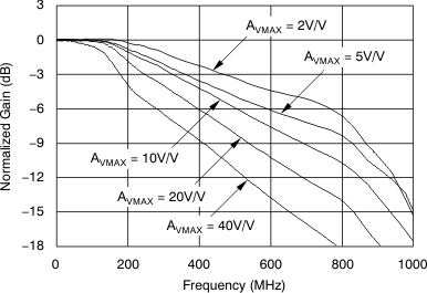 Figure 77. SOIC-14 Recommended RF and RG vs AVMAX
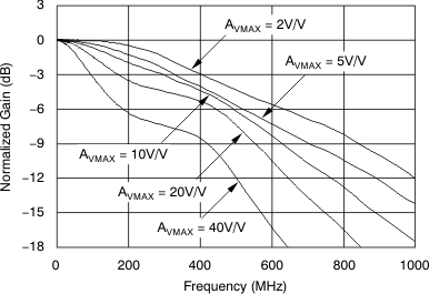 Figure 78. VSSOP-10 Recommended RF and RG vs AVMAX
10.2 Typical Applications
10.2.1 Wideband Variable-Gain Amplifier Operation Application
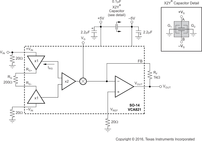 Figure 79. DC-Coupled, AVMAX = 20 dB, Bipolar Supply Specification and Test Circuit
10.2.1.1 Design Requirements
The design shown in Figure 79 requires a single-ended input, continuously variable gain control and a single-ended output. This configuration is used to achieve the best performance with a bipolar supply. This circuit also requires a maximum gain of 10 V/V and low noise.
10.2.1.2 Detailed Design Procedure
The VCA821 device provides an exceptional combination of high output power capability with a wideband, greater than 40-dB gain adjust range, linear in dB variable gain amplifier. The VCA821 device input stage places the transconductance element between two input buffers, using the output currents as the forward signal. As the differential input voltage rises, a signal current is generated through the gain element. This current is then mirrored and gained by a factor of two before reaching the multiplier. The other input of the multiplier is the voltage gain control pin, VG. Depending on the voltage present on VG, up to two times the gain current is provided to the transimpedance output stage. The transimpedance output stage is a current-feedback amplifier providing high output current capability and high slew rate, 2500 V/μs. This exceptional full-power performance comes at the price of relatively high quiescent current (34 mA), but low input voltage noise for this type of architecture (6 nV/√Hz).
Figure 79 shows the DC-coupled, gain of +10 V/V, dual power-supply circuit used as the basis of the ±5-V Electrical Characteristics and Typical Characteristics. For test purposes, the input impedance is set to 50 Ω with a resistor to ground and the output impedance is set to 50 Ω with a series output resistor. Voltage swings reported in the Electrical Characteristics table are taken directly at the input and output pins, while output power (dBm) is at the matched 50-Ω load. For the circuit in Figure 79, the total effective load is 100 Ω ∥ 1 kΩ.
NOTE
For the SOIC-14 package, there is a voltage reference pin, VREF (pin 9). For the SOIC-14 package, this pin must be connected to ground through a 20-Ω resistor in order to avoid possible oscillations of the output stage. In the VSSOP-10 package, this pin is internally connected and does not require such precaution.
An X2Y® capacitor has been used for power-supply bypassing. The combination of low inductance, high resonance frequency, and integration of three capacitors in one package (two capacitors to ground and one across the supplies) enables the VCA821 device to achieve the low second-harmonic distortion reported in the Electrical Characteristics table. More information on how the VCA821 device operates can be found in the Operating Suggestions section.
10.2.1.3 Application Curve
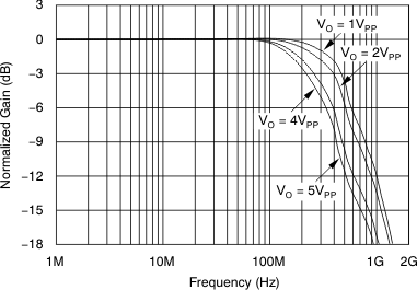 Figure 80. Large-Signal Frequency Response
10.2.2 Difference Amplifier Application
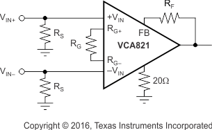 Figure 81. Difference Amplifier
10.2.2.1 Design Requirements
For a difference amplifier, the design requirements are differential voltage gain, common mode rejection, and load drive capability. This circuit delivers differential gain of 2* (Rf/Rg), and CMRR as shown in Figure 82.
10.2.2.2 Detailed Design Procedure
Because both inputs of the VCA821 device are high-impedance, a difference amplifier can be implemented without any major problem. Figure 81 shows this implementation. This circuit provides excellent common-mode rejection ratio (CMRR) as long as the input is within the CMRR range of –2.1 V to +1.6 V.
NOTE
This circuit does not make use of the gain control pin, VG. Also, it is recommended to choose RS such that the pole formed by RS and the parasitic input capacitance does not limit the bandwidth of the circuit.
Figure 82 shows the common-mode rejection ratio for this circuit implemented in a gain of 20 dB for VG = +2 V.
NOTE
Because the gain control voltage is fixed and is normally set to +2 V, the feedback element can be reduced to increase the bandwidth. When reducing the feedback element, make sure that the VCA821 device is not limited by common-mode input voltage, the current flowing through RG, or any other limitation described in this data sheet.
10.2.2.3 Application Curve
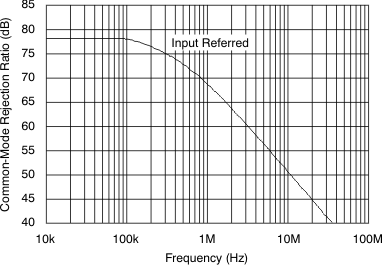 Figure 82. Common-Mode Rejection Ratio
10.2.3 Differential Equalizer Application
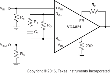 Figure 83. Differential Equalizer
10.2.3.1 Design Requirements
Signals that travel over a length of cable experience an attenuation that is proportional to the square root of the frequency. For this reason, a fixed bandwidth amplifier will not restore the original signal. To replicate the original signal, the higher frequency signal components require more gain. The circuit in Figure 83 has one stage of frequency shaping to help restore a signal transmitted along a cable. If needed, additional frequency shaping stages can be added as shown in Figure 84.
10.2.3.2 Detailed Design Procedure
If the application requires frequency shaping (the transition from one gain to another), the VCA821 device can be used advantageously because its architecture allows the application to isolate the input from the gain setting elements. Figure 83 shows an implementation of such a configuration. The transfer function is shown in Equation 5.
This transfer function has one pole, P1 (located at RGC1), and one zero, Z1 (located at R1C1). When equalizing an RC load, RL and CL, compensate the pole added by the load located at RLCL with the zero Z1. Knowing RL, CL, and RG allows the user to select C1 as a first step and then calculate R1. Using RL = 75 Ω, CL = 100 pF and wanting the VCA821 device to operate at a gain of +2 V/V (which gives RF = RG = 453 Ω) allows the user to select C1 = 15.5 pF to ensure a positive value for the resistor R1. With all these values known, to achieve greater than 300-MHz bandwidth, R1 can be calculated to be 20 Ω. Figure 84 shows the frequency response for both the initial, unequalized frequency response and the resulting equalized frequency response.

10.2.3.3 Application Curve
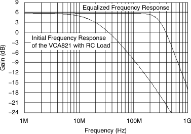 Figure 84. Differential Equalization of an RC Load
10.2.4 Differential Cable Equalizer Application
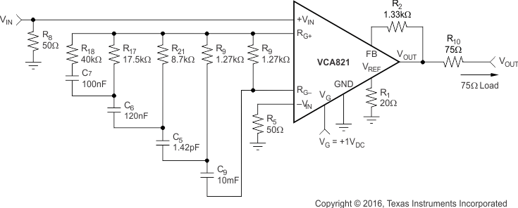 Figure 85. Differential Cable Equalizer
10.2.4.1 Design Requirements
Signals that travel over a length of cable experience an attenuation that is proportional to the square root of the frequency. For this reason, a fixed bandwidth amplifier will not restore the original signal. To replicate the original signal, the higher frequency signal components require more gain. The circuit in Figure 85 has multiple stages of frequency shaping to help restore a signal transmitted along a cable. This circuit is similar to the one shown in Figure 83, but is much more accurate in replicating the 1/(sqrt(f)) frequency response shape.
10.2.4.2 Detailed Design Procedure
A differential cable equalizer can easily be implemented using the VCA821 device. An example of a cable equalization for 100 feet of Belden cable 1694F is illustrated in Figure 84, with Figure 86 showing the result for this implementation. This implementation has a maximum error of 0.2 dB from DC to 70 MHz.
NOTE
This implementation shows the cable attenuation side-by-side with the equalization in the same plot.
For a given frequency, the equalization function realized with the VCA821 device matches the cable attenuation. The circuit in Figure 85 is a driver circuit. To implement a receiver circuit, the signal is received differentially between the +VIN and –VIN inputs.
10.2.4.3 Application Curve
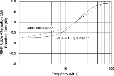 Figure 86. Cable Attenuation vs Equalizer Gain
10.2.5 AGC Loop Application
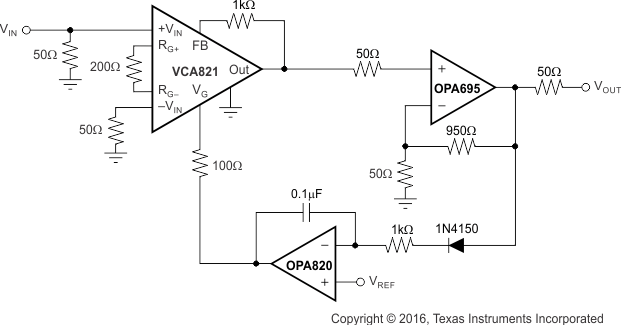 Figure 87. AGC Loop
10.2.5.1 Design Requirements
When dynamic signal amplitude correction is required, an AGC loop will provide real-time gain control. The requirements for this circuit are fast gain control response and linear in dB gain control. The time constant of the loop is set with the 0.1-µF capacitor and the 1-kΩ resistor. The OPA695 provides additional load driving capability.
10.2.5.2 Detailed Design Procedure
In the typical AGC loop shown in Figure 87, the OPA695 device follows the VCA821 device to provide 40 dB of overall gain. The output of the OPA695 device is rectified and integrated by an OPA820 device to control the gain of the VCA821 device. When the output level exceeds the reference voltage (VREF), the integrator ramps down reducing the gain of the AGC loop. Conversely, if the output is too small, the integrator ramps up increasing the net gain and the output voltage.
10.3 System Examples
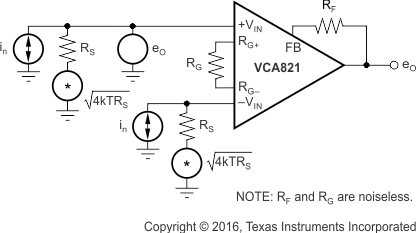 Figure 88. Simple Noise Model
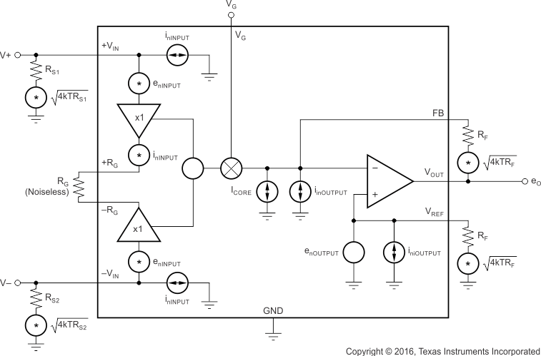 Figure 89. Full Noise Model