SBOS407D December 2007 – May 2016 VCA821
PRODUCTION DATA.
- 1 Features
- 2 Applications
- 3 Description
- 4 Revision History
- 5 Device Comparison Table
- 6 Pin Configuration and Functions
-
7 Specifications
- 7.1 Absolute Maximum Ratings
- 7.2 ESD Ratings
- 7.3 Recommended Operating Conditions
- 7.4 Thermal Information
- 7.5 Electrical Characteristics: VS = ±5 V
- 7.6 Typical Characteristics: VS = ±5 V, DC Parameters
- 7.7 Typical Characteristics: VS = ±5 V, DC and Power-Supply Parameters
- 7.8 Typical Characteristics: VS = ±5 V, AVMAX = 6 dB
- 7.9 Typical Characteristics: VS = ±5 V, AVMAX = 20 dB
- 7.10 Typical Characteristics: VS = ±5 V, AVMAX = 32 dB
- 8 Parameter Measurement Information
- 9 Detailed Description
- 10Application and Implementation
- 11Power Supply Recommendations
- 12Layout
- 13Device and Documentation Support
- 14Mechanical, Packaging, and Orderable Information
1 Features
- 710-MHz Small-Signal Bandwidth
(G = +2 V/V) - 320 MHz, 4 VPP Bandwidth (G = +10 V/V)
- 0.1-dB Gain Flatness to 135 MHz
- 2500 V/μs Slew Rate
- > 40-dB Gain Adjust Range
- High Gain Accuracy: 20 dB ±0.3 dB
- High Output Current: ±90 mA
2 Applications
- AGC Receivers With RSSI
- Differential Line Receivers
- Pulse Amplitude Compensation
- Variable Attenuators
- Voltage-Tunable Active Filters
3 Description
The VCA821 device is a DC-coupled, wideband, linear in dB, continuously variable, voltage-controlled gain amplifier. It provides a differential input to single-ended conversion with a high-impedance gain control input used to vary the gain down 40 dB from the nominal maximum gain set by the gain resistor (RG) and feedback resistor (RF).
The VCA821 device internal architecture consists of two input buffers and an output current feedback amplifier stage integrated with a multiplier core to provide a complete variable gain amplifier (VGA) system that does not require external buffering. The maximum gain is set externally with two resistors, providing flexibility in designs. The maximum gain is intended to be set between 6 dB and 32 dB. Operating from ±5-V supplies, the gain control voltage for the VCA821 device adjusts the gain linearly in dB as the control voltage varies from 0V to +2 V. For example, set at a maximum gain of 20 dB, the VCA821 device provides 20 dB, at VG = +2 V, to less than –20 dB at VG = 0 V. The VCA821 device offers excellent gain linearity. For a 20-dB maximum gain, and a gain-control input voltage varying between +1 V and +2 V, the gain does not deviate by more than ±0.3 dB (maximum at +25°C).
Device Information(1)
| PART NUMBER | PACKAGE | BODY SIZE (NOM) |
|---|---|---|
| VCA821 | SOIC (14) | 8.65 mm × 3.91 mm |
| VSSOP (10) | 3.00 mm × 3.00 mm |
- For all available packages, see the orderable addendum at the end of the data sheet.
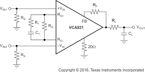
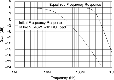
Differential Equalizer

Differential Equalization of an RC Load
