ZHCSKG7B June   2019  – February 2024 UCC5390-Q1

PRODUCTION DATA  

  1.   1
  2. 特性
  3. 应用
  4. 说明
  5. Pin Configuration and Function
  6. Specifications
    1. 5.1  Absolute Maximum Ratings
    2. 5.2  ESD Ratings
    3. 5.3  Recommended Operating Conditions
    4. 5.4  Thermal Information
    5. 5.5  Power Ratings
    6. 5.6  Insulation Specifications for DWV Package
    7. 5.7  Safety-Related Certifications For DWV Package
    8. 5.8  Safety Limiting Values
    9. 5.9  Electrical Characteristics
    10. 5.10 Switching Characteristics
    11. 5.11 Insulation Characteristics Curves
    12. 5.12 Typical Characteristics
  7. Parameter Measurement Information
    1. 6.1 Propagation Delay, Inverting, and Noninverting Configuration
      1. 6.1.1 CMTI Testing
  8. Detailed Description
    1. 7.1 Overview
    2. 7.2 Functional Block Diagram
    3. 7.3 Feature Description
      1. 7.3.1 Power Supply
      2. 7.3.2 Input Stage
      3. 7.3.3 Output Stage
      4. 7.3.4 Protection Features
        1. 7.3.4.1 Undervoltage Lockout (UVLO)
        2. 7.3.4.2 Active Pulldown
        3. 7.3.4.3 Short-Circuit Clamping
    4. 7.4 Device Functional Modes
      1. 7.4.1 ESD Structure
  9. Application and Implementation
    1. 8.1 Application Information
    2. 8.2 Typical Application
      1. 8.2.1 Design Requirements
      2. 8.2.2 Detailed Design Procedure
        1. 8.2.2.1 Designing IN+ and IN– Input Filter
        2. 8.2.2.2 Gate-Driver Output Resistor
        3. 8.2.2.3 Estimate Gate-Driver Power Loss
        4. 8.2.2.4 Estimating Junction Temperature
      3. 8.2.3 Selecting VCC1 and VCC2 Capacitors
        1. 8.2.3.1 Selecting a VCC1 Capacitor
        2. 8.2.3.2 Selecting a VCC2 Capacitor
        3. 8.2.3.3 Application Circuits With Output Stage Negative Bias
      4. 8.2.4 Application Curve
  10. Power Supply Recommendations
  11. 10Layout
    1. 10.1 Layout Guidelines
    2. 10.2 Layout Example
    3. 10.3 PCB Material
  12. 11Device and Documentation Support
    1. 11.1 Device Support
      1. 11.1.1 第三方产品免责声明
    2. 11.2 Documentation Support
      1. 11.2.1 Related Documentation
    3. 11.3 Certifications
    4. 11.4 接收文档更新通知
    5. 11.5 支持资源
    6. 11.6 Trademarks
    7. 11.7 静电放电警告
    8. 11.8 术语表
  13. 12Revision History
  14. 13Mechanical, Packaging, and Orderable Information

封装选项

机械数据 (封装 | 引脚)
散热焊盘机械数据 (封装 | 引脚)
订购信息

CMTI Testing

Figure 6-3 is a simplified diagram of the CMTI testing configuration.
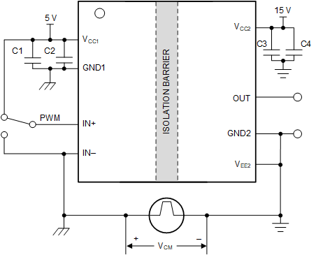
GUID-843EB2D8-67D4-4CDE-8742-501D452F9D2E-low.gif Figure 6-3 CMTI Test Circuit for UCC5390-Q1