ZHCSPH5C June 2022 – March 2023 UCC28C50 , UCC28C51 , UCC28C52 , UCC28C53 , UCC28C54 , UCC28C55 , UCC28C56H , UCC28C56L , UCC28C57H , UCC28C57L , UCC28C58 , UCC28C59 , UCC38C50 , UCC38C51 , UCC38C52 , UCC38C53 , UCC38C54 , UCC38C55
PRODUCTION DATA
9.2.2.2 变压器匝数比和最大占空比
变压器的设计首先是为给定应用选择合适的开关频率。UCC28C42 能够以最高 1MHz 的频率开关,但通常需要考虑转换器的总体尺寸、开关损耗、磁芯损耗、系统兼容性以及对通信频带的干扰等因素来确定应使用的最佳频率。对于该离线转换器,将开关频率 (fSW) 选择为 110kHz 作为折衷方案,从而尽可能地减小变压器尺寸和 EMI 滤波器尺寸,同时仍然具有可接受的损耗。
变压器的初级与次级匝数比 (NPS) 可以根据所需的 MOSFET 额定电压和次级二极管额定电压来选择。由于最大输入电压为 265VRMS,因此可以按照方程式 4 所示计算峰值体输入电压。

为了尽可能地减少系统的成本,选择了一种现成的 650V MOSFET。将漏极上的最大电压应力降额至其额定值的 80%,并允许漏电感电压尖峰达到最大体输入电压的 30%,反射输出电压必须小于 130V,如方程式 5 所示。

12V 输出的最大初级与次级变压器匝数比 (NPS) 可以选择为:

设计示例中使用了 NPS = 10 的匝数比。
辅助绕组用于向控制器提供偏置电压。导通后偏置电压需要保持在 VDD 最小工作电压以上,以保证系统稳定工作。此设计中为控制器选择的最小 VDD 工作电压为 10V。选择辅助绕组以支持 12V 的偏置电压,使其高于最低工作电平,但仍保持 IC 中的低损耗。初级与辅助匝数比 (NPA) 可根据方程式 7 进行计算:

输出二极管承受的电压应力等于输出电压加上反射的输入电压:

TI 建议使用额定阻断电压大于 60V 的肖特基二极管,以应对振铃引起的电压尖峰。该二极管的正向压降 (VF) 估计为 0.6V
为了避免高峰值电流,本设计中的反激式转换器在连续导通模式下工作。确定 NPS 后,就可以使用 CCM 反激式转换器的传递函数来计算最大占空比 (DMAX):

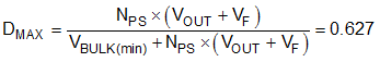
由于最大占空比超过 50%,且该设计为离线(交流输入)应用,因此 UCC28C42 最适合此应用。