ZHCSPH5C June 2022 – March 2023 UCC28C50 , UCC28C51 , UCC28C52 , UCC28C53 , UCC28C54 , UCC28C55 , UCC28C56H , UCC28C56L , UCC28C57H , UCC28C57L , UCC28C58 , UCC28C59 , UCC38C50 , UCC38C51 , UCC38C52 , UCC38C53 , UCC38C54 , UCC38C55
PRODUCTION DATA
- 1 特性
- 2 应用
- 3 说明
- 4 Revision History
- 5 Device Comparison Table
- 6 Pin Configuration and Functions
- 7 Specifications
-
8 Detailed Description
- 8.1 Overview
- 8.2 Functional Block Diagram
- 8.3
Feature Description
- 8.3.1 Detailed Pin Description
- 8.3.2 Undervoltage Lockout
- 8.3.3 ±1% Internal Reference Voltage
- 8.3.4 Current Sense and Overcurrent Limit
- 8.3.5 Reduced-Discharge Current Variation
- 8.3.6 Oscillator Synchronization
- 8.3.7 Soft-Start Timing
- 8.3.8 Enable and Disable
- 8.3.9 Slope Compensation
- 8.3.10 Voltage Mode
- 8.4 Device Functional Modes
-
9 Application and Implementation
- 9.1 Application Information
- 9.2
Typical Application
- 9.2.1 Design Requirements
- 9.2.2
Detailed Design Procedure
- 9.2.2.1 Input Bulk Capacitor and Minimum Bulk Voltage
- 9.2.2.2 Transformer Turns Ratio and Maximum Duty Cycle
- 9.2.2.3 Transformer Inductance and Peak Currents
- 9.2.2.4 Output Capacitor
- 9.2.2.5 Current Sensing Network
- 9.2.2.6 Gate Drive Resistor
- 9.2.2.7 VREF Capacitor
- 9.2.2.8 RT/CT
- 9.2.2.9 Start-Up Circuit
- 9.2.2.10 Voltage Feedback Compensation
- 9.2.3 Application Curves
- 9.3 Power Supply Recommendations
- 9.4 Layout
- 10Device and Documentation Support
- 11Mechanical, Packaging, and Orderable Information
7.6 Typical Characteristics
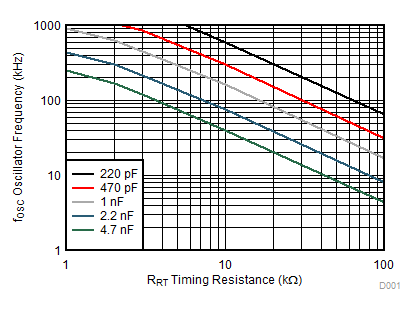 Figure 7-1 Oscillator Frequency vs Timing Resistance and Capacitance
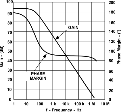 Figure 7-3 Error Amplifier Frequency Response
| Group 1: UCCx8C50 to UCCx8C55 | Group 2: UCC28C56H/L, UCC28C57H/L, and UCC28C58/9 |

| Group 1: UCCx8C50 to UCCx8C55 | Group 2: UCC28C56H/L, UCC28C57H/L, and UCC28C58/9 |
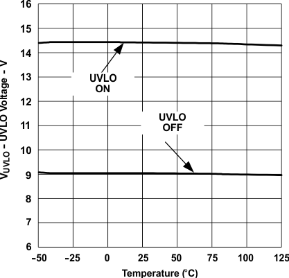
| UCCx8C52 and UCCx8C54 |
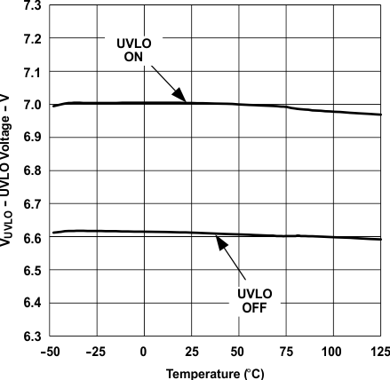
| UCCx8C50 and UCCx8C51 |

| UCC28C56L and UCC28C57L |
 Figure 7-15 Supply Current vs Oscillator Frequency
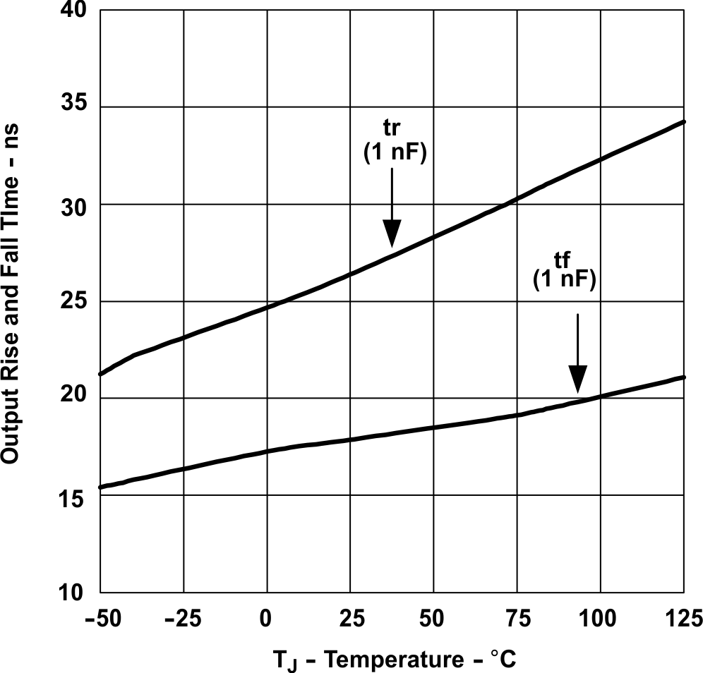 Figure 7-17 Output Rise Time and Fall Time vs Temperature
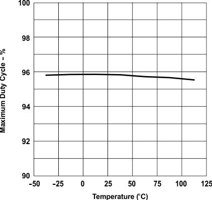 Figure 7-19 Maximum Duty Cycle vs Temperature
| Group 1: UCCx8C50 to UCCx8C55 | Group 2: UCC28C56H/L, UCC28C57H/L, and UCC28C58/9 |

| Group 1: UCCx8C50 to UCCx8C55 | Group 2: UCC28C56H/L, UCC28C57H/L, and UCC28C58/9 |

| VCS = 0 V | |
| Group 1: UCCx8C50 to UCCx8C55 | Group 2: UCC28C56H/L, UCC28C57H/L, and UCC28C58/9 |

| Group 1: UCCx8C50 to UCCx8C55 | Group 2: UCC28C56H/L, UCC28C57H/L, and UCC28C58/9 |
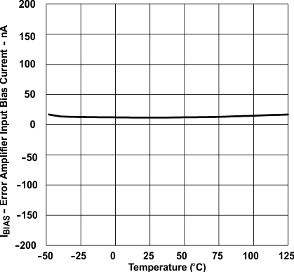 Figure 7-8 Error Amplifier Input Bias Current vs Temperature
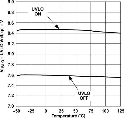
| UCCx8C53 and UCCx8C55 |

| UCC28C56H and UCC28C57H |

| UCC28C58 and UCC28C59 |

| Group 1: UCCx8C50 to UCCx8C55 | Group 2: UCC28C56H/L, UCC28C57H/L, and UCC28C58/9 |
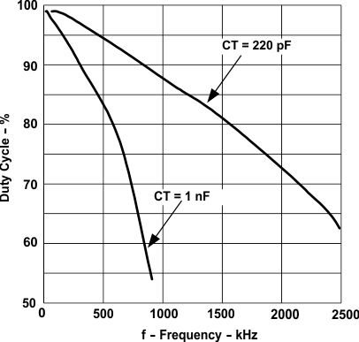 Figure 7-18 Maximum Duty Cycle vs Oscillator Frequency
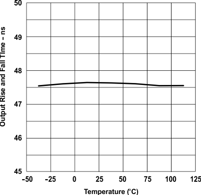 Figure 7-20 Maximum Duty Cycle vs Temperature
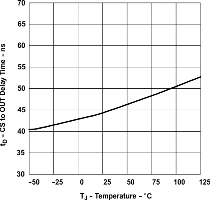 Figure 7-22 Current Sense to Output Delay Time vs Temperature