ZHCSPH5C June 2022 – March 2023 UCC28C50 , UCC28C51 , UCC28C52 , UCC28C53 , UCC28C54 , UCC28C55 , UCC28C56H , UCC28C56L , UCC28C57H , UCC28C57L , UCC28C58 , UCC28C59 , UCC38C50 , UCC38C51 , UCC38C52 , UCC38C53 , UCC38C54 , UCC38C55
PRODUCTION DATA
- 1 特性
- 2 应用
- 3 说明
- 4 Revision History
- 5 Device Comparison Table
- 6 Pin Configuration and Functions
- 7 Specifications
-
8 Detailed Description
- 8.1 Overview
- 8.2 Functional Block Diagram
- 8.3
Feature Description
- 8.3.1 Detailed Pin Description
- 8.3.2 Undervoltage Lockout
- 8.3.3 ±1% Internal Reference Voltage
- 8.3.4 Current Sense and Overcurrent Limit
- 8.3.5 Reduced-Discharge Current Variation
- 8.3.6 Oscillator Synchronization
- 8.3.7 Soft-Start Timing
- 8.3.8 Enable and Disable
- 8.3.9 Slope Compensation
- 8.3.10 Voltage Mode
- 8.4 Device Functional Modes
-
9 Application and Implementation
- 9.1 Application Information
- 9.2
Typical Application
- 9.2.1 Design Requirements
- 9.2.2
Detailed Design Procedure
- 9.2.2.1 Input Bulk Capacitor and Minimum Bulk Voltage
- 9.2.2.2 Transformer Turns Ratio and Maximum Duty Cycle
- 9.2.2.3 Transformer Inductance and Peak Currents
- 9.2.2.4 Output Capacitor
- 9.2.2.5 Current Sensing Network
- 9.2.2.6 Gate Drive Resistor
- 9.2.2.7 VREF Capacitor
- 9.2.2.8 RT/CT
- 9.2.2.9 Start-Up Circuit
- 9.2.2.10 Voltage Feedback Compensation
- 9.2.3 Application Curves
- 9.3 Power Supply Recommendations
- 9.4 Layout
- 10Device and Documentation Support
- 11Mechanical, Packaging, and Orderable Information
9.1 Application Information
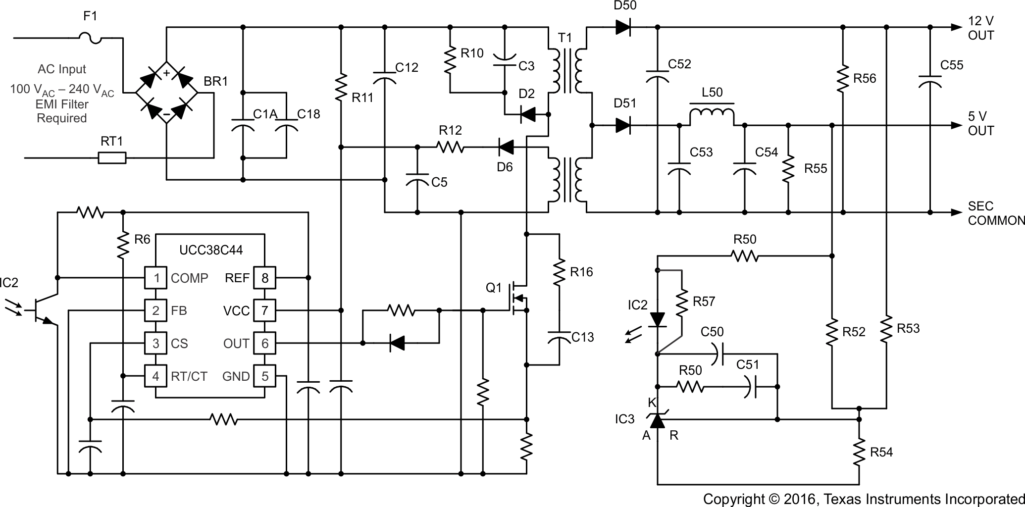
The UCC28C5x controllers are peak current mode pulse width modulators. These controllers have an onboard amplifier and can be used in isolated and nonisolated power supply designs. The onboard totem pole gate driver is capable of delivering 1 A of peak current. This high-speed PWM is capable of operating at switching frequencies up to 1 MHz. Since UCCx8C5x can be used to directly substitute UCCx8C4x by drop-in, the design steps are the same as those for UCCx8C4x. The same design example, including the layout, of UCCx8c4x is re-used for UCCx8C5x as shown below.Figure 9-1 shows a typical off-line application using UCC38C44.
 Figure 9-1 Typical Off-Line Application
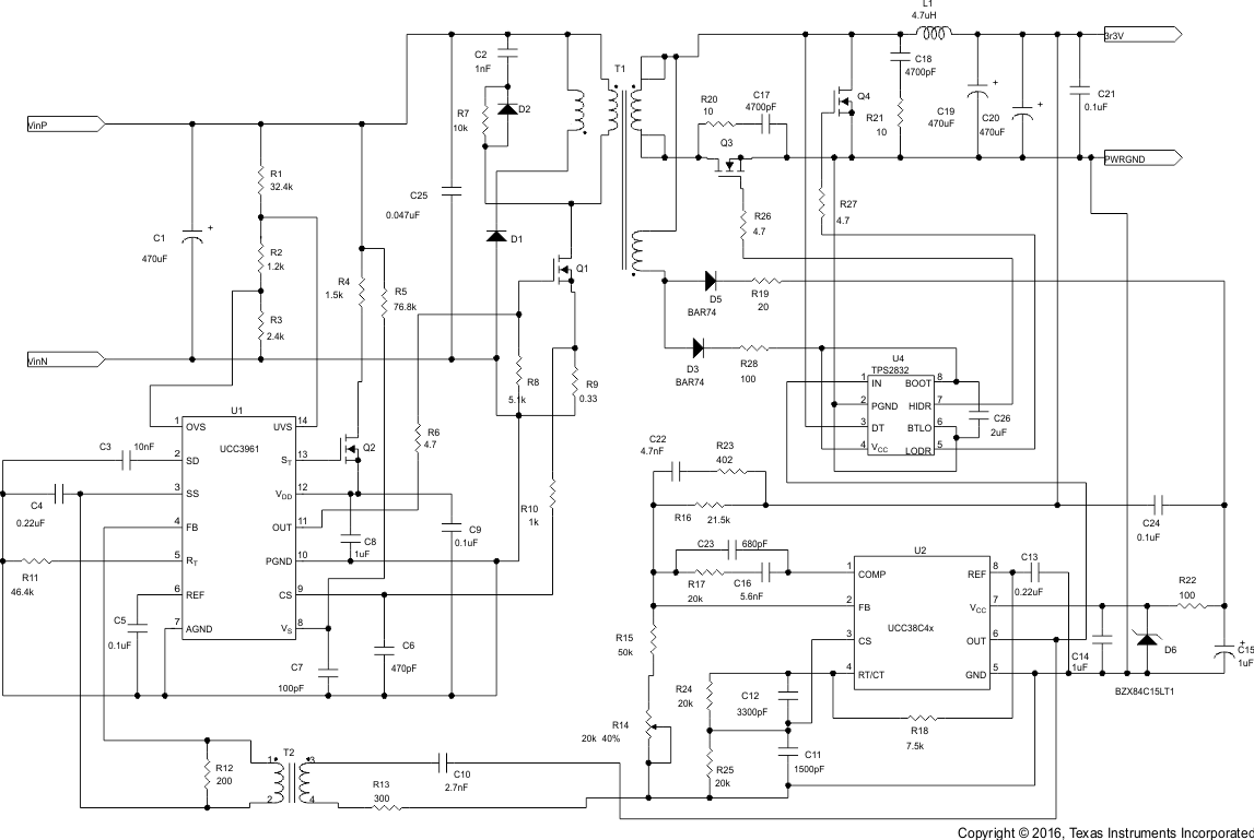
Figure 9-2 shows a forward converter with synchronous rectification. This application provides 48 V to 3.3 V at 10 A with over 85% efficiency, and uses the UCC38C42as the secondary-side controller and UCC3961 as the primary-side startup control device.
 Figure 9-2 Forward Converter with Synchronous Rectification Using the UCC38C42 as the Secondary-Side Controller