ZHCSBB1D July   2013  – March 2018 UCC28740

PRODUCTION DATA.  

  1. 特性
  2. 应用
  3. 说明
    1.     Device Images
      1.      简化应用示意图
      2.      典型伏安图
  4. 修订历史记录
  5. Pin Configuration and Functions
    1.     Pin Functions
  6. Specifications
    1. 6.1 Absolute Maximum Ratings
    2. 6.2 ESD Ratings
    3. 6.3 Recommended Operating Conditions
    4. 6.4 Thermal Information
    5. 6.5 Electrical Characteristics
    6. 6.6 Switching Characteristics
    7. 6.7 Typical Characteristics
  7. Detailed Description
    1. 7.1 Overview
    2. 7.2 Functional Block Diagram
    3. 7.3 Feature Description
      1. 7.3.1 Detailed Pin Description
      2. 7.3.2 Valley-Switching and Valley-Skipping
      3. 7.3.3 Startup Operation
      4. 7.3.4 Fault Protection
    4. 7.4 Device Functional Modes
      1. 7.4.1 Secondary-Side Optically Coupled Constant-Voltage (CV) Regulation
      2. 7.4.2 Primary-Side Constant-Current (CC) Regulation
  8. Application and Implementation
    1. 8.1 Application Information
    2. 8.2 Typical Application
      1. 8.2.1 Design Requirements
      2. 8.2.2 Detailed Design Procedure
        1. 8.2.2.1 Custom Design With WEBENCH® Tools
        2. 8.2.2.2 Standby Power Estimate and No-Load Switching Frequency
        3. 8.2.2.3 Input Bulk Capacitance and Minimum Bulk Voltage
        4. 8.2.2.4 Transformer Turns-Ratio, Inductance, Primary Peak Current
        5. 8.2.2.5 Transformer Parameter Verification
        6. 8.2.2.6 VS Resistor Divider, Line Compensation
        7. 8.2.2.7 Output Capacitance
        8. 8.2.2.8 VDD Capacitance, CVDD
        9. 8.2.2.9 Feedback Network Biasing
      3. 8.2.3 Application Curves
  9. Power Supply Recommendations
  10. 10Layout
    1. 10.1 Layout Guidelines
      1. 10.1.1 VDD Pin
      2. 10.1.2 VS Pin
      3. 10.1.3 FB Pin
      4. 10.1.4 GND Pin
      5. 10.1.5 CS Pin
      6. 10.1.6 DRV Pin
      7. 10.1.7 HV Pin
    2. 10.2 Layout Example
  11. 11器件和文档支持
    1. 11.1 器件支持
      1. 11.1.1 开发支持
        1. 11.1.1.1 使用 WEBENCH® 工具定制设计方案
      2. 11.1.2 器件命名规则
        1. 11.1.2.1  电容术语(以法拉为单位)
        2. 11.1.2.2  占空比术语
        3. 11.1.2.3  频率术语(以赫兹为单位)
        4. 11.1.2.4  电流术语(以安培为单位)
        5. 11.1.2.5  电流和电压调节术语
        6. 11.1.2.6  变压器术语
        7. 11.1.2.7  功率术语(以瓦特为单位)
        8. 11.1.2.8  电阻术语(以 Ω 为单位)
        9. 11.1.2.9  时序术语(以秒为单位)
        10. 11.1.2.10 电压术语(以伏特为单位)
        11. 11.1.2.11 交流电压术语(以 VRMS 为单位)
        12. 11.1.2.12 效率术语
    2. 11.2 文档支持
      1. 11.2.1 相关文档
    3. 11.3 接收文档更新通知
    4. 11.4 社区资源
    5. 11.5 商标
    6. 11.6 静电放电警告
    7. 11.7 Glossary
  12. 12机械、封装和可订购信息

封装选项

机械数据 (封装 | 引脚)
散热焊盘机械数据 (封装 | 引脚)
订购信息

Typical Application

The UCC28740 is well suited for use in isolated off-line systems requiring high efficiency and fault protection features such as USB compliant adapters and chargers for consumer electronics such a smart phones, tablet computers, and cameras. A 10-W application for a USB charger is shown in Figure 18.

This procedure outlines the steps to design a constant-voltage, constant-current flyback converter using the UCC28740 controller. See Figure 18 for component names and network locations. The design procedure equations use terms that are defined below.
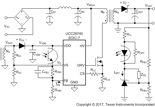
UCC28740 ai_apxmpl_lusbf3.gifFigure 18. Design Procedure Application Example